
Now that the “technology bricks” for building 2.5D devices and 3D ICs have been essentially qualified, the focus has turned to optimizing them for improved cost of ownership (CoO). At last week’s European 3D TSV Summit, in Grenoble, France, many of the supplier presentations demonstrated how their companies have been working to optimize qualified 3D TSV technologies across the process flow.
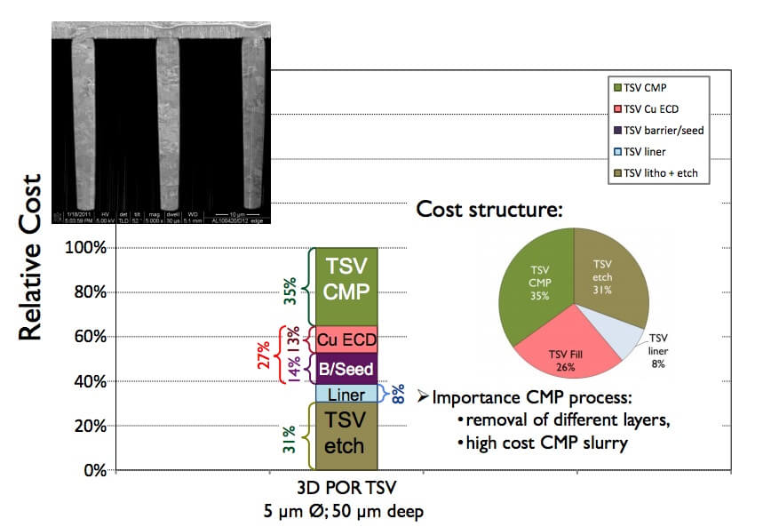
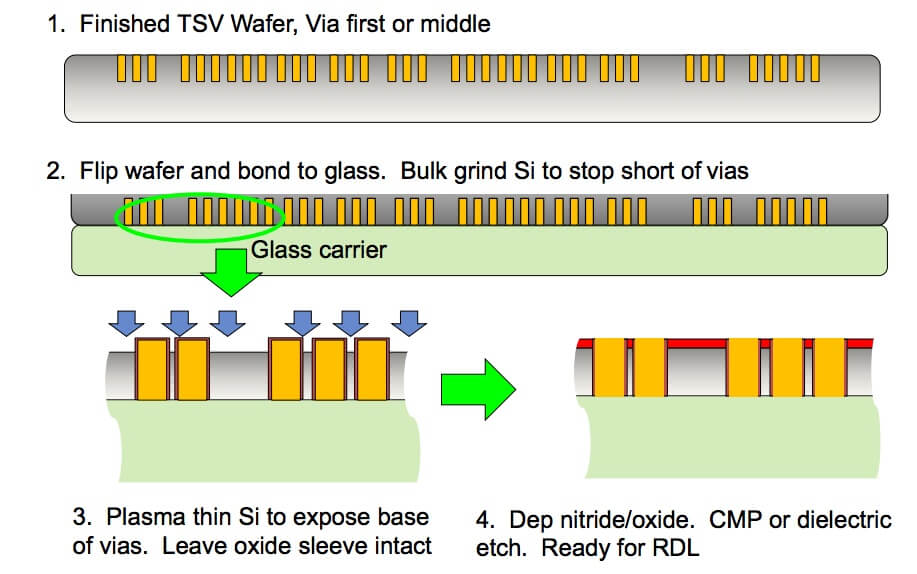
Eric Beyne got the ball rolling talking about imec’s process of record (POR) for the via-mid TSVs, resulting in vias with an aspect ratio of 10, based on 5µm diameter and 50µm depth, and how efforts to scale TSVs in either direction can affect CoO. The secret lies in the etch process. Beyne explained how accurate TSV etch improves liner quality and TSV reliability, reduces required TSV depth, and allows for CMP-less thin wafer backside process. He pointed out that 35% of the cost is in the chemical mechanical planarization (CMP) step, and that cost savings can be achieved trying do to without CMP and lithography processes, and instead using wet etch and self alignment. (Figure 1).
eyne also talked about temporary bond and debond (TB/DB), and the subsequent wafer thinning, backside passivation, and via reveal steps as critical cost savings areas. Imec has settled on room-temperature peel debondable carrier systems, or as he called it “the magic post-it at the wafer-level”, and that more equipment and materials suppliers are engaging, leading to cost reduction and performance improvements.
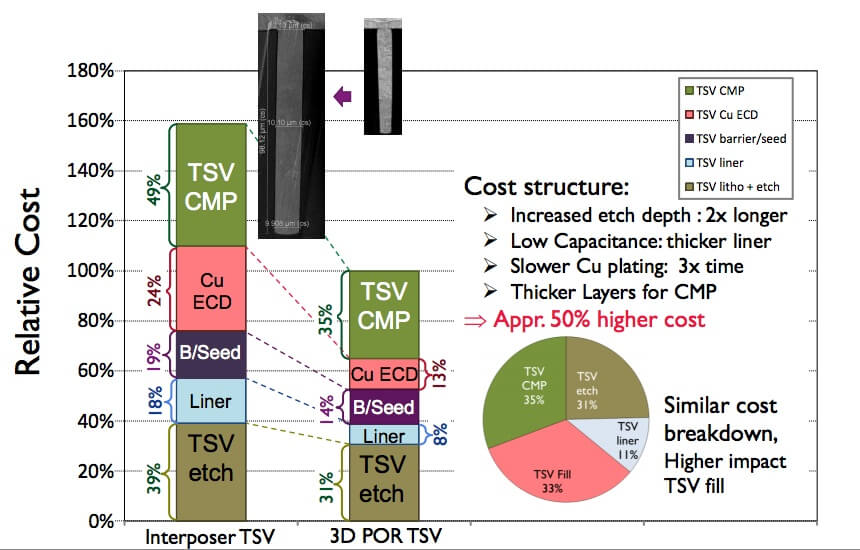
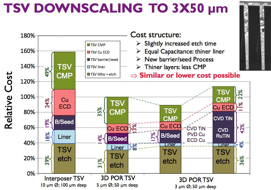
With regard to scaling TSVs, there are technology advantages and disadvantages in both directions. Ultimately, interposers scaled up to 10×100µm realize a 50% cost increase over 5×50µm (Figure 2). Whereas downscaling to 3×50µm may offer a cost savings (Figure 3).
By far the most challenging step in the backside process flow has been one that precedes the actual processes: TB/DB. But things are finally looking up thanks to the diligent efforts and collaboration between the equipment and materials suppliers to solve these issues. Indeed, during presentations from SUSS MicroTec, EV Group, and Brewer Science, the equipment manufacturers tipped their hats to the materials guys and vice versa, for finally achieving (according to Ron Huemoeller of Amkor) 100% debond yields.
Tony Flaim, of Brewer Science, explained how the company has reformulated its thermoplastic bonding material to allow for single-coat application, which when combined with process improvements resulted in a better total thickness variation (TTV). Through collaborative efforts with research centers (imec and ITRI) and equipment suppliers, they determined how to better match the device wafer and bonding material surface energies. In determining the cause of stress patterns or wrinkling after PECVD, what was originally perceived as a material failure was fixed by process and equipment changes. Additionally, controlling the polymer structure and using a blend to achieve synergistic rheological properties allowed for viscoelastic properties to be stabilized at higher temperatures.
Now, if we could only get the CoO down. In his presentation, Rinehardt Knippelmeyer of SUSS MicroTec talked about lessons learned bringing 2.5D interposer technologies into production. He said room temperature debonding is the only process that fulfills all the base criteria necessary for industrialization. The next step is preparing processes and materials for high volume manufacturing. He said the challenges the industry is facing with bringing new temporary bonding processes into production are intrinsic and involve thermal stability, chemical stability, and dealing with particles. Knipplemeyer said next steps for SUSS involve extending the process latitude, qualifying new materials, taking materials that are in manufacturing and extending them further, and enhancing the debonding concept, all in an effort to improve CoO.
According to Paul Lindner, EV Group is already progressing down the road of reduced CoO with the introduction of its production platform targeting high volume manufacturing HVM). The tool features nine process modules vs. four, and double the number of FOUP loading ports over the earlier generation platform. It also features in situ metrology for measuring total thickness variation TTV. Lindner says this has resulted in “equipment induced” CoO reduction of >50%. On the materials side, Lindner noted that thinner adhesives enable lower CoO and also provide better TTV and a more stable TSV manufacturing process.
Next on the checklist for CoO optimization are the backside processes themselves: thinning, passivation and via reveal. David Butler, SPTS and Laura Mauer, SSEC, duked it out on the wet vs. dry etch debate, each presenting compelling processes that include proprietary end-point detection functionalities.
While Beyne pointed to wet etch with CMP replaced by a “fine grind” process step as a possible path to cost reduction, Butler stood firmly behind SPTS’s dry etch and via reveal featuring end-point detection as the preferred course of action. He said wet etch chemistries are “nasty” and that to date, none of SPTS customers have wet etch on their roadmap.
Butler walked us through a simple process flow for the via reveal step (figure 4). After the grind step, how much silicon remains above the via is uncertain. And since each wafer is different, a pass through a profilometer offline is required, adding time and often leading to re-work which adds to the cost. End point detection avoids all that, eliminating the need for rework and ultimately saves money.

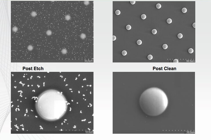
Offering the wet etch perspective, Mauer said wet wafer thinning for via reveal is “all about minimizing costs.” SSEC has developed a low-cost wet etch process with integrated metrology for performing thickness measurement and end point detection.
The ‘secret sauce’ of this process is potassium hydroxide (KOH) as the etchant chemistry, which Mauer explained exposes the via without etching the oxide liner or having and effect of the copper. This is followed by a sealing step with low temperature oxide/nitride, and a final CMP step to planarize and expose the vias. This process flow requires fewer overall steps than a plasma process, which Mauer explained leads to cost savings. KOH does require a cleaning process, which is incorporated into SSEC’s tool (Figure 5). Mauer says she believes that integrated process control and recirculating the chemistry leads to a lower CoO.
Depositing a barrier and seed layer is another critical step in the TSV metallization scheme, and while costly, PVD has remained the preferred method of performing this process. Glyn Reynolds of Oerlikon Systems talked about the advantages and disadvantages of PVD, and how the company is addressing the disadvantages – high cost, energy inefficiencies and poor sidewall coverage – with its novel process, highly ionized sputtering (HIS). In a nutshell, HIS reduces the cost of directional PVD by implementing high current, short cycle pulses that create high-density plasma right at the target. This way, enough material is deposited into deep vias with vertical sidewalls. Reynolds noted that HIS results in improved performance, while reducing CoO thanks to:
- Higher throughput
- Lower cost of consumables
- Lower power consumption
- Less cooling water required
- Higher target utilization
- Longer target life/ increased time between target changes
- Simple, inexpensive shield design
Finally, we come to the chip stacking processes themselves. Lindner and Hannes Kostner, of Besi, both talked about the ongoing collaboration with EVG and Besi on their advanced chip to wafer process, which involves an integrated system for die placement followed by a permanent collective bond.
With a solid background in HVM flip chip bonders, Besi is leveraging that core competency to develop a thermocompression die bonder that meets the requirements for stacking TSV die such as thin die handling, accuracy, coplanarity and bond control. Kostner reported that the first tool buyoff was successful with a first time dual head/single pass assembly of multilayer TSV stacks at 50µ die thickness. The second evaluation is currently underway, and 27 companies have decided to use TCB technology “sooner or later.”
I found the mere presence of Besi at the TSV Summit to be significant, because it signifies that we are on the path to HVM. “We had to see a HVM application before committing development costs in to high volume tool,” explained Kostner. “Wide I/O DRAM is that application.”
So there you have it. Progress is clearly being made and I expect future charts at subsequent events to show lower CoO is happening. Stay tuned for more on the European 3D TSV Summit. ~ F.v.T.


