
At the 2023 IMAPS Symposium in October, I had some great community member conversations about some of the hot topics of the day. They shared their opinions on everything from the possibility of the U.S. onshoring advanced packaging technology in high volumes, to the impact of germanium and gallium restrictions on the compound semiconductor development, to the recent announcement by Intel on the introduction of glass core substrates for next-generation advanced packaging, and much more.
John Lannon and Rex Anderson, Micross Components, talk about the companies’ expansions over the past few years to build out their products and services to support high-reliability markets. Photonics is a growth area for the company, and they are working with companies to develop co-packaged optics solutions using 3D integration technologies. Lannon and Anderson also helped demystify the multiple government funding efforts to onshore advanced packaging, and how Micross is being impacted by these efforts.

Casey Krawiec of StratEdge Corporation talks about the company’s role in delivering packaging technology for high-frequency applications, the growth in high-reliability sectors, and why 2023 will go down as a good year for StratEdge. He explains the impact of restricted materials such as germanium, gallium, and Kovar on their supply chains.
Brian Schmaltz, Namics Corporation, talks about the company’s efforts to eliminate harmful PFAS chemicals from their portfolio of products. He also explains the Environmental Protection Agency’s (EPAs) expectations for PFAS reporting by chemical companies for the last 10 years, and the company audits that are expected.

Understanding how much PFAS is out there can help determine the next steps. Namics is already adapting ahead of requirements to become PFAS-free. The company provides underfill epoxies, conductive adhesives, films, and liquid adhesives for advanced packaging. Namics is a Japanese company that has environmental efforts embedded in its very name: Nature, Art, Mutual prosperity, Innovation, Creativity, and Sensitivity.

Vahid Akhavan, PulseForge explains how the company’s core competency — high-powered photonic-based pulsed light technology — is being used for temporary bond/debond processes for everything from fan-out, interposer, and chiplet integration, to LEDs and high-power applications. Current debonding approaches rely on columnated laser technology to ash adhesive bonding materials. The PulseForge approach uses a broad spectrum, high-powered pulsed light to replace laser, for a cleaner and higher throughput debond step. The company works with integrators like ERS Electronic GmbH to deliver fully automated temporary debonding solutions.
Ajinomoto Fine Techno’s Habib Hichri talked about developments beyond its core ABF (Ajinomoto Buil-up Film) to meet the needs of next-generation thin and large packages. He detailed one material in development that is used for both dielectric as well as mold compound used in fan-out panel level packaging that reduces warpage.
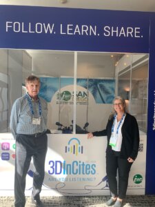
QP Technologies’ CEO Dick Otte, returns to the podcast to talk about his impressions of this year’s event, and to explain why QP has decided to NOT pursue CHIPS for America Act funding. He says he’s spent months analyzing the situation and has concluded that CHIPS Act Funding is designed for the “big guys”. It will only provide 30% of the money needed to expand an onshore facility, much of that through tax incentives. After weighing that against the task of raising the other 70% of funding required for an expansion of QP, he has decided to wait and see how it all plays out.
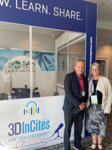
Paul Ballentine, co-founder of Mosaic Microsystems, talks about the growing enthusiasm around using glass technology in microelectronics manufacturing. He explains how one of the challenges with glass was a lack of supply chain. Describing Mosaic as a “supply chain company”, he talks about his involvement with the U.S. Government in building out the advanced packaging cluster in Rochester New York.
Peter Cronin, MRSI Systems, talked about the company’s latest foray into die-bonding tools – the MRSI 705 HF machine, that delivers 50kg of force for high force bonding applications, such as medical applications. He came to IMAPS to learn more about advancements in co-packaged optics, chiplets, and heterogeneous integration. MRSI submitted proposals to participate in some of the Microelectronics Commons programs.
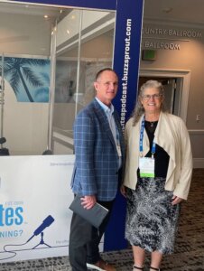
I wrapped up the day chatting over drinks with Onto Innovation’s Keith Best. He talked about being inspired by Bill Chen’s heterogeneous integration roadmap (HIR) presentation. Bill shared the history of microelectronics industry roadmapping, dating back to Fairchild Semiconductor and the ITRS. He stressed the importance of bringing the community together to make things happen. We also talked about the IMAPS organization itself, and how much we enjoy the camaraderie of IMAPS events.
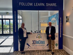
Lastly, we discussed the implications of Intel’s announcement that they’ve developed a glass core substrate technology for next-generation advanced packaging to replace other materials being used, such as copper-clad laminate.
You can get the full story by listening to the podcast here.


![[err-ad-fallback-title]](http://www.3dincites.com/wp-content/plugins/a3-lazy-load/assets/images/lazy_placeholder.gif)


