


As semiconductor devices are subject to increasingly higher quality and reliability standards, extensive measures must be taken to ensure these standards are met. At the same time, new highly integrated, complex packaging solutions – including a variety of new materials and structures – are being adopted to achieve the economic and performance advantages that were previously met with silicon scaling. These factors call for the use of highly advanced tools to analyze potential failures, which often require physical access to the die. Obtaining unambiguous results in failure analysis strongly depends on the quality of sample preparation, such as selective removal of the encapsulant material while preserving the bond wires, re-distribution metal, bond pads, passivation, die, and the original failure sites.
Conventional Approaches to Decapsulation
Due to the stacking structure and relatively small, package-to-die size ratio, the decapsulation of complex 3D stacked-die packages appears to be very challenging when using conventional techniques involving acids or carbon tetrafluoride (CF4) based reactive ion etch (RIE) systems. The latter two techniques have intrinsic limitations, which are especially apparent in advanced packages that include 3D structures.
Conventional acid decapsulation can easily damage the top layer die and bond wires due to overexposure to acid, while the middle and bottom layer structures remain unexposed. It is also quite challenging to preserve the package perimeter to perform further electrical tests in specific test sockets when using acid decapsulation. The feature photo above compares a 26mmx29mm SiP module after acid decapsulation (left) and after MIP decapsulation. The image labeled ‘Acid indicates the over-etching and corrosion damage induced by acid decapsulation of a system-in-package (SiP) module.
Using conventional CF4-based reactive ion etch (RIE) decapsulation makes it even more difficult to reach the middle and bottom layer structures due to the thick molding compound layer and stepwise structure. Also, CF4 often causes over-etching damage to the passivation layer and the silicon die, as these materials are readily etched in fluorine plasma. The high energy ion bombardment in the commonly used RIE plasma systems can damage the electrical functionality of the device, preventing further analysis steps. To summarize: The use of acid or CF4-based plasma decapsulation methods can induce damage or alteration of original structures, and possibly introduce corrosion, over-etching, and foreign contamination reducing analysis accuracy and confidence levels during root cause failure analysis. [1]
Microwave Induced Plasma Decapsulation
To overcome the limitations of conventional decapsulation techniques and enable artifact-free sample preparation, a fully automatic decapsulation machine has been developed based on a novel, low-power (P<100W) atmospheric pressure microwave-induced plasma (MIP). The highly confined plasma beam of the MIP tool results in a high flux of neutral oxygen radicals in the plasma afterglow, contributing to the high molding compound etch rate and high etch selectivity of common wire bond materials like gold, silver, and copper, and Si die. As has been previously reported, the atmospheric pressure oxygen-only MIP etching can achieve high selectivity of mold compound to wire/pad/passivation/die. [2] The absence of ion bombardment and microwave stray fields is crucial to prevent damaging the device inside the package. It has been shown that semiconductor devices remain fully functional after their packages have been decapsulated using the MIP tool.
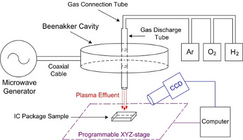
The MIP tool consists of a low-power microwave generator (2450 MHz), a custom-built Beenakker-type microwave resonant cavity, a gas discharge tube, mass flow controllers, a camera, a programmable XYZ-stage, cleaning unit, and drying unit (Figure 2).
The MIP process is carried out in two steps. During the first step, the epoxy in the molding compound is selectively removed by high-density oxygen radicals in the MIP effluent beam that is scanned across the sample surface. The remaining agglomerate layer of silicon dioxide filler particles is removed in an ultrasonic deionized water bath during the second step. This etch-clean-dry cycle is repeated, enabling layer-by-layer removal of epoxy mold compound while the functional components and the original failure sites in the package are preserved. [3]
Figure 3 illustrates the described MIP decapsulation process flow. Sample preparation is not necessarily required before MIP processing. However, to optimize the process and reduce overall decapsulation time, it is helpful to remove bulk mold compounds above the top wire loops using laser ablation or milling methods. Figure 3a shows a package after laser ablation, which is then etched by MIP in Figure 3b, and cleaned in deionized water in Figure 3c to remove the filler particles. [4]


The etching chemistry and subsequent high selectivity of the MIP decapsulation process remove the risk of overreaching and facilitate the removal of the packaging material while ensuring that the bond wires, bond pads, dies, original structures, and failure sites are preserved in an excellent state. The image labeled MIP in Figure 1 illustrates artifact-free exposure of all active and passive devices in a SiP module using MIP. Figure 4 shows more detailed images of a decapsulated 3D structure on the SiP module.


Using MIP for 2.5D Package Decapsulation
As part of the MIP tool’s continuous application development, the focus has recently been placed on 2.5D packages, proving that the MIP process selectively removes organic materials, such as epoxy mold compound, underfill or polyimide, on a die or in-between two dies on the 2.5D package to enable further analysis steps. Cu micro-bump, solder joint, die pad exposure (top-down or cross-section exposure) on 2.5D interposer die or 3D NAND dies are areas where MIP shows its unique capabilities compared to conventional decapsulation techniques.
Interposer interconnects, for example, are difficult to expose using conventional decapsulation methods, because the laminate, chip bumps, and µbumps would be attacked by wet chemicals. Fluorocarbon-based plasma etchers will attack the passivation, metal layers, and chip silicon. Contrary to that, the atmospheric pressure MIP is a highly selective and isotropic process and can expose interposer interconnects while preserving all materials and original failures sites, allowing for subsequent, careful analysis.
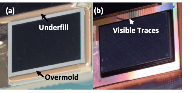
Using the atmospheric pressure MIP process to remove underfill over or around 2.5D structures does not alter all other materials on the samples. µBumps can also be cleanly exposed either from the top down or in a cross-section (Figure 5), enabling analysis of defects further into the cross-section, while guaranteeing that no artifacts are induced by the sample preparation. [5]


Figure 5. a) MIP processing exposed the first row of µpillars in a cross-section and b) MIP process was able to expose the second row into the sample where the first µpillar row was mechanically polished into.
Removing the packaging material between closely spaced chips on a silicon interposer is quite challenging. MIP’s ability to remove the packaging material from these very high aspect ratio spaces allows inspection of the conductive traces in the silicon interposer in this area of high risk of interconnect failure (Figure 6).
The atmospheric pressure MIP system is a unique tool for artifact-free decapsulation to enable undisputable identification of failures. The system’s high etching selectivity, speed, and repeatability enable complex advanced packaging decapsulation, ensuring a high success rate of the related failure analyses and reliability investigations.
References
1. J. Tang, M. R. Curiel, S. L. Furcone, E. G. J. Reinders, C. T. . Revenberg, and C. I. M. Beenakker, ‘Failure analysis of complex 3D stacked-die IC packages using Microwave Induced Plasma afterglow decapsulation’, in 2015 IEEE 65th Electronic Components and Technology Conference (ECTC), 2015.
2. Ibid.
3. C. Odegard, A. Burnett, J. Tang, J. Wang, ‘Preserving Evidence for Root Cause Investigations with Halogen-Free Microwave Induced Plasma Decapsulation’, in Proceedings 44th International Symposium for Testing and Failure Analysis, 2018.
4. Ibid
5. K. Distelhurst, J. Myers, D. Bader, P. Pichumani, J. Tang, M. McKinnon, “Analysis of 2.5D Module after Underfill Removal with a CF4-Free Microwave Induced Plasma (MIP) Spot Etch Process”, to be published at International Symposium for Testing and Failure Analysis, 2020.


