


On May 20 MEPTEC’s Executive Director, Ira Feldman, moderated another informative MEPTEC & iMAPS webinar. Two Knowledgeable speakers from Ansys and International Test Solutions (ITS) outlined their company’s technical capabilities and explained the value these tools and methodologies provide for multi-die IC design and test.
Modeling and Simulation of Multi-die IC Designs
Sooyong Kim, Sr Product Manager for 3DIC CPS (Chip-Package-System) delivered Ansys’ presentation, titled “Multi-disciplinary Simulation for 2.5D/3DIC Co-Design”. He gave a great overview, showing the value of electronic design automation (EDA) tools (Figure 1) then focused on Ansys’ broad range of modeling and simulation tools for 2.5D building blocks and chip – package – system co-design.
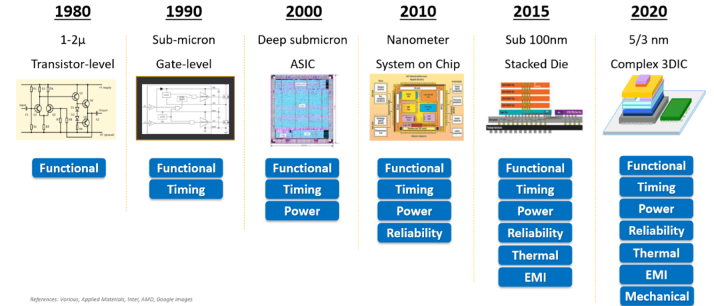
Kim explained that several decades ago, the functionality of designs with tens of transistors could simply be implemented and verified manually by experienced humans. Today’s multi-die IC designs include many millions of transistors, even may contain tens of billions of transistors and take 100s of person-months and many millions of dollars to develop.
Personal comment: This slide should give people who still think “I have a lot of experience and can rely on prototyping” some food for thought. Building in enough margin “to make it work without using EDA tools” is not practical anymore, nor economical. Exhaustive multi-physics verification with the right EDA tools, using accurate models of building blocks as inputs, is the fastest and lowest-cost path to success.
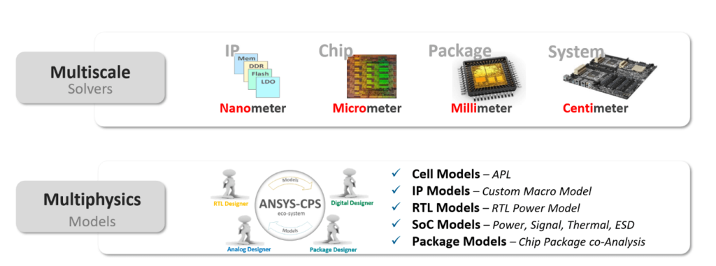
In Figure 2, Kim highlighted that Ansys offers solvers for a wide range of dimensions: from nanometers for transistors to centimeters for system-level simulations. This slide also emphasizes the importance of accurate models, to get meaningful simulation results and lists several models Ansys tools can generate, as foundations for accurate and comprehensive multi-physics simulations, at different abstraction levels.
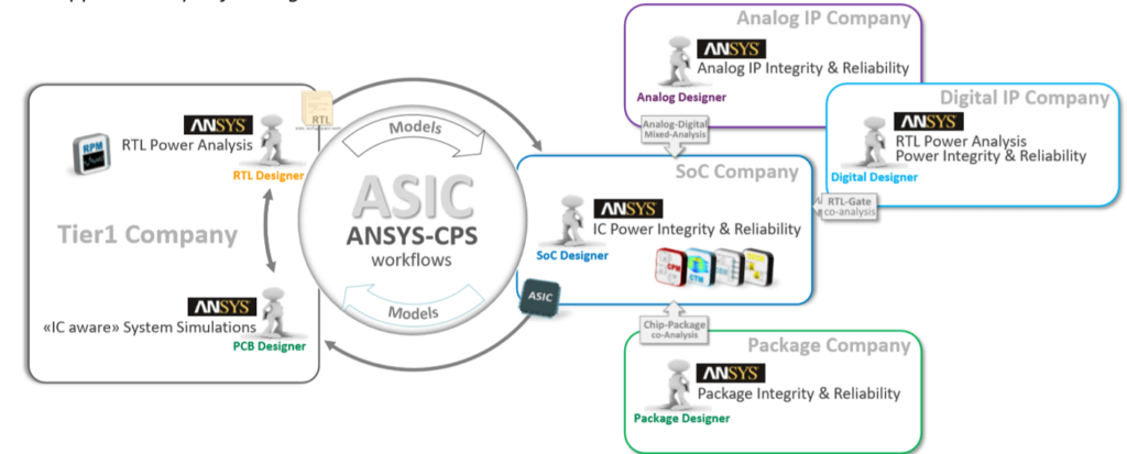
In addition to many technical topics, Kim also addressed the value of Ansys; chip-package-system capabilities within the electronic supply chain. Figure 3 shows Ansys tools in this context and emphasizes again the importance of modeling and simulation of multi-physics building blocks.
After giving this overview of multi-disciplinary design challenges, Kim presented and explained several 2.5D design examples that showed how Ansys tools and methodologies address power integrity (PI), electrical-thermal-mechanical interactions, and Signal Integrity (SI). His entire presentation has been recorded and can be viewed here.
Multi-die IC Test
The second speaker, Jerry Broz, SVP of Technology Development at International Test Solutions (ITS) in Reno, demonstrated his company’s contribution to cleaning wafer probe-cards, also outlined how ITS cleans test sockets for fully packaged units.
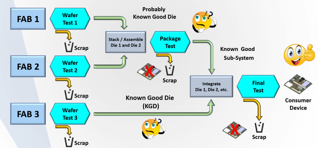
Because the final yield of a multi-die IC is the product of all building blocks’ yields (BB1 yield x BB2 yield x BB3 ….), very thorough probing of every die is essential – to achieve high-yielding multi-die IC devices. Known good die (KGD), (a.k.a. probably good die) are extremely important yield criteria for multi-die ICs and raise the importance of in-depth probing (without reporting any false positives or negatives) of every die. See a basic multi-die IC test flow in Figure 4.
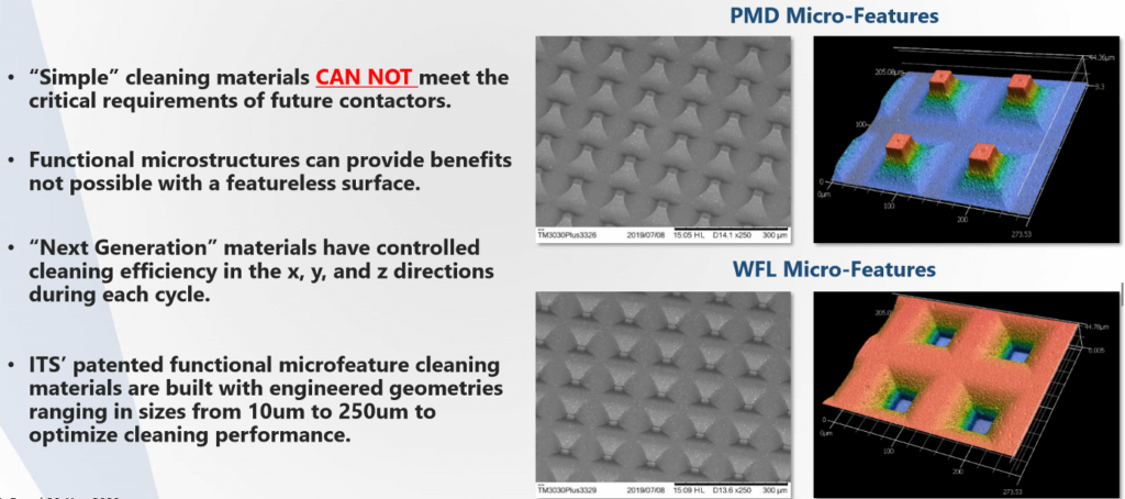
Because the tightly-spaced (~ 40µm currently) and tiny probe-tips of MEMS-based probe cards can only exert a small force (1 gram or less) to make contact with the wafer and can easily be contaminated, frequent cleaning of such probe-cards is mandatory. Traditional cleaning materials, with non-functionalized surfaces cannot achieve thorough enough cleaning. ITS developed functional cleaning materials to clean every probe-tip individually (Figure 5).
To substantiate the value of ITS advanced probe-card cleaning techniques, Broz showed several actual yield statistics, comparing results with and without cleaning of probe tips.
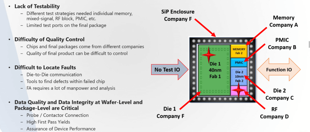
Broz also addressed another multi-die IC challenge: When integrating heterogeneous functions, the wafers are typically coming for different fab, specifying different probe requirements – see Figure 6 – and also demanding customization of the functionalized cleaning materials, before wafer probing can be ramped up.
See/listen to Broz’s entire presentation here.
Personal comment: The list of topics in Figure 6 clearly points out that best practices and standards need to be agreed upon and published, to make heterogeneous integration easier to implement and more cost-effective. To address these challenges, several major industry organizations started the Heterogeneous Integration Roadmap (HIR) efforts. See more about HIR background, mission, and other important topics at SEMI’s HIR home page here.
After discussing in-depth how ITS contributes to improving wafer-probing, Broz outlined that ITS also offers cleaning solutions for test sockets. Test sockets for ICs with thousands, even tens of thousands of contact points, need to be also perfectly clean to enable high-quality final tests of fully assembled single-die SoCs and multi-die ICs.
Personal Comments for Both Presentations
I am still fascinated by all the ideas and solutions experienced engineering experts can contribute to making 2.5/3D-IC technologies easier to use and more cost-effective.
- Kim’s presentation demonstrates Ansys’ support for high-complexity, multi-die IC designs, especially for important co-design challenges, like PI, SI, and thermal considerations, with Ansys modeling and simulation tools.
- Broz’s message changed my perspective of KGD. In my mind it is now no longer an oxymoron, “only” a significant challenge innovative engineers are working on solving. I look forward to the Known Good Die Workshop on September 16 to get a lot of information about this important topic.
What will MEPTEC and iMAPS offer next?
On Wednesday, June 17:
- Stephen Rothrock from ATREG will present: US-China Trade War – The Tariff Effects on the Global OSAT Market.
- Chris Barratt from Insight SIP will address: Design of Miniature Multi-Mode SiP Modules with Two Integrated Antennas
On Wednesday, July 15, Jan Vardaman from TechSearch International will give a Global Market Update.
On Wednesday, September 16, will be the full day Known Good Die Workshop at SEMI in Milpitas. See more about it here.
Thanks for reading…Herb


