While the focus of IFTLE remains on the latest advances in advanced chip packaging, we have mentioned before that we must also stay on top of peripheral technologies since they are required to use our advanced packaging. For instance, what good are advanced packages if there are no advanced printed circuit boards (PCBs) on which to mount them?
The April issue of PCB Circuit Design and Fab / Circuits Assembly contains an interesting article by Todd MacFaddan, of Bose, entitled “BGA Pitch Impact on Bare Board Fabrication Detailing the Impact of Package Complexity on PCB Complexity.”
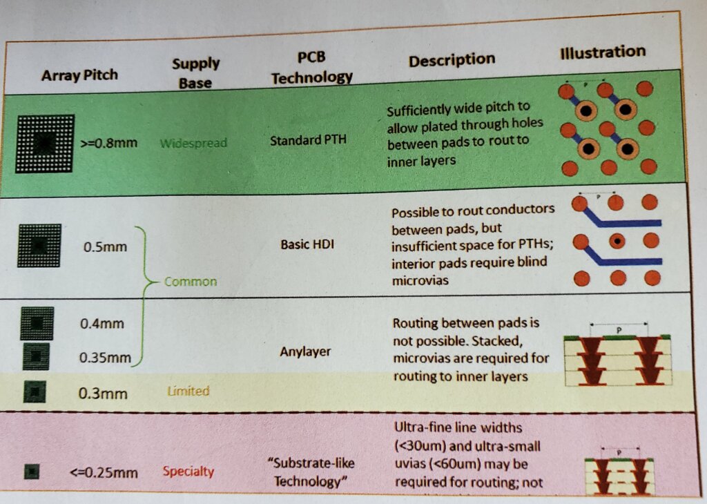
We all know that high IO packaging has evolved from peripheral IO to area array, and from ball grid arrays (BGAs) to chip-scale package (CSPs), wafer-level CSP, and flip-chips, defined by a steady march toward smaller balls at a finer pitch (Figure 1).

Array pitch has profound implications for the PCB industry, which must continually develop newer methods to route every coming generation of high-I/O packages with increasingly finer pitch. In fact, it is argued by the author that the pitch of array packages has been the most important driver in PCB technology developments, and will continue to be for the foreseeable future. As area array package pitch continues to shrink to accommodate chip density, the number of PCB suppliers with the capability to fabricate PCBs to support these finer pitches decreases (Figure 2).

This article discusses the impact of sub 0.4mm pitch on PCB fabrication in relation to laser drill, laminate type, stack-up, patterning (etch), solder mask, and test. A few of their conclusions follow.
Laser Drilling
With pitch < 0.4mm, it is generally not possible to route between pads. Therefore, via-in-pad is required to escape inner array pins to inner layers. A 0.3mm pitch array typically requires a 75µm via, which is often the lower limit of most conventional CO2 lasers. Below 0.3mm pitch, smaller holes are needed, which generally require UV lasers which, while more accurate and cleaner, are slower and thus more costly. In addition, there are reliability concerns with stacked µvias 75µm and smaller, particularly when stacked four or more high they are reportedly much more susceptible to pad lifting during reflow processing and suffer premature failure.
Materials
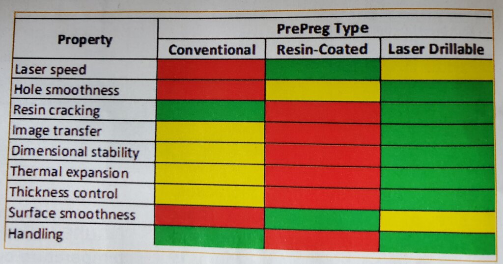
The non-homogeneity of standard PCB laminate materials yields rough, inconsistent laser-drilled holes with poor size and location accuracy. Resin-coated copper (RCC) which does not use fiberglass, was developed to solve this problem. While RCC materials dramatically improved laser drill quality they were expensive, difficult to handle, and had poor dimensional stability, thus they are no longer common. More recently alternate fiberglass materials with a flattened weave pattern have been developed to facilitate consistent hole shape and accuracy during laser drill, without changing the resin-glass ratio making the creation of small µvias possible (Figure 3).

Stack-up
Because there is insufficient space to route conductors between interior pads of fine-pitch arrays, µvias must be used for routing these rows to inner layers (Figure 4). For full arrays, this usually requires any layer construction, in which blind µvias can be used on any layer, thereby providing full routing freedom. The larger the array, the more layers are required for routing.

With traditional high-density interconnect (HDI) construction, the core layer is usually a fully cured rigid copper-clad laminate and forms structural support during fabrication. But with any layer technology, there is no traditional “core” layer for support, and the thin starting layers are fragile and not compatible with conventional processes. Any layer technology, therefore, requires suppliers to invest in specialized processes and equipment to fabricate coreless stack-ups and thin buildup layers, such as horizontal etching, vertical continuous plating, automated loading/unloading robots and other techniques to minimize processing and handling damage.
Buildup technology used in any layer construction requires sequential processing, whereby each buildup layer must be processed through all of 10 to 15 steps sequentially. High-volume any-layer technology requires tremendous capital investment, particularly in bottleneck processes such as drilling and lamination where redundant equipment is essential to maintain volume capacity.
Patterning
<0.3mm pitch devices typically requires interconnect line widths below 60 to 75µm which in turn generally require laser direct imaging (LDI) because standard photo tools introduce too much variation due to alignment and resolution imperfections. Additive processes must be used for such ultra-fine lines. The most common type is modified semi-additive patterning. In this process, dry film is used to mask non-pattern areas, and the desired conductor pattern is exposed to electroplating. Thus, the pattern is built up rather than etched down.
In conclusion, the ever-decreasing pitch of advanced packages directly impacts most key PCB fabrication processes and requires significant capital investments.
For all the latest in Advanced Packaging stay linked to IFTLE……………………….


