Ever since I put on the editorial director hat for 3D-ICs.com, which aggregates 3D technology news, blogs and papers, and categorizes them as either TSV and 3D packaging or monolithic 3D, I’ve been trying to wrap my head around the differences between 3D TSVs and monolithic 3D integration technologies. I’ve got 2.5 D and 3D TSVs down pat, but the monolithic thing was really eluding me. I decided the best course of action was to tap into an expert in the monolithic realm. Who better to talk to than Zvi Or-Bach, CEO of MonilithIC 3D? I figured if his company carries the technology name, he must know the most about it. I wasn’t disappointed. Or-Bach graciously explained it all to me, right down to the fundamentals. Now that I’ve got it all straightened out, I figured 3D InCites readers could benefit from this knowledge as well.
The Fundamentals
According to Or-Bach, there are two fundamental differences between 3D TSVs and monolithic 3D (also known as 3D sequential integration); how they are manufactured, and the physical difference in the end device.
3D TSVs involve taking two finished device wafers (either from the same or different fabs) and vertically interconnecting them at the chip level with through silicon vias (TSVs) in either wafer-to-wafer or die-to-wafer processes. Process steps are generally grouped and are named front-end-of-line (FEOL), middle-of-the-line (MOL) and back-end-of-line (BEOL), and may be performed at different locations (foundry and OSAT, for example). Many of the MOL process steps require new equipment.
Monolithic 3D wafers are manufactured all in one fab, and rather than stacking 2 or more wafers, you start with a base wafer onto which additional layers of crystallized silicon and metalized layers are added using traditional fab equipment.The vertical interconnects are formed between layers rather than chips, using vias in the nanometer rather than micron range. Rather than calling these TSVs, explained Or-Bach, they are really through layer vias (TLVs).
The second fundamental difference lies in the end-device of these processes. “The difference in manufacturing translates into difference in the device,” notes Or-Bach. As mentioned, TSV 3D stacks require two wafers, and thinning of one of the wafers. TSVs are 5-10µm and wafer pairs are a minimum of 50µm. “In 3D TSV, the end device is measured in microns, which is very limited,” he explained. “You can connect full functions, as long as you don’t need too many connections. “
On the other hand, with monolithic, you never have second wafer, but rather a 100nm layer of crystallized silicon, which results in a multiple order of magnitude of difference in both the size of the vias and the final device size. In this case, you’re dealing with nanometers rather than microns. The end device will be smaller and thinner, interconnection is 10,000 times higher due to the number of vertical connections. Additionally, as transistors are measured in nanometers not microns, with monolithic 3D you end up with a vertical connectivity that is comparable to horizontal connectivity.
Or-Bach explained how the 3D structures look completely different. “In the case of TSV we stack together elements that if without TSV would need to be interconnected side by side on a printed circuit board. There are lots of advantages to this such as, saving area, and the power required to run a signal from one chip, through the PCB to another chip.” He explained. “In monolithic 3D, we start with a device that used to be 10×10µm in 2D that is now 5×5µm in two layers.” 3D TSV interconnect is between chips. Monolithic 3D is on-chip interconnect.
It’s important to not confuse monolithic 3D with what ITRI’s John Lau calls 3D silicon. 3D silicon still uses 2 wafers, but rather than using microbumps as is the case with 3D TSV stacking, the wafers are bonded first and then the vias are formed, and are at the 5µm size. Like monolithic 3D, 3D silicon is also a foundry based manufacturing process, but Or-Bach says the vertical via densities are not anywhere close to the high levels provided by monolithic 3D.
Monolithic 3D: Not a New Concept
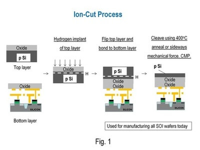
According to Or-Bach, the industry has been talking conceptually about monolithic 3D for over 30 years. The brick wall was always the thermal limitation. Once copper is involved to form the interconnect, there is a limitation to heating the wafer beyond 400°C. Beyond that temperature the interconnect reliability greatly degrades. Yet, building up layers with crystallized silicon requires heating to 1000°C. Over the last 20 years, researchers gave up trying to find a solution around it and settled on TSVs as the way to go. “We didn’t accept that, and kept searching for a solution,” explained Or –Bach, referring to his company MonolithIC 3D. “We found a way to build the layers without exceeding the 400°C limits of copper.” Basically, they developed and patented a process that uses high temperature when the silicon is not on top of the copper, and then use a layer transfer process and cold processes to finish the job. The processed is based on the ion-cut process used to manufacture SOI wafers (Fig 1).

Adoption Timeline for 3D Integration
Experts say 2.5D products using passive silicon interposers are going into HVM now, and 3D ICs will follow in 2013. When it comes to 3D silicon, Lau predicts adoption to not happen until 2020 because of the cost involved and the processes yet to be ironed out. According to Or-Bach, versions of monolithic 3D could come to market in 2013-2014 in the NAND flash industry because it provides a cost effective alternative to scaling, which is reaching its limits. Instead of building a 1gigabyte device, we’re building 2 gigabytes for the same cost. All of a sudden, scaling can be done in the 3D rather than 2D and achieve the required performance improvements in a smaller footprint.
“Monolithic is more about how we can integrate the device. We use lithography to make next nodes, which presents a different manufacturing challenge than TSVs do. In the end we believe that it’s cheaper than scaling,” he says.
Key Applications
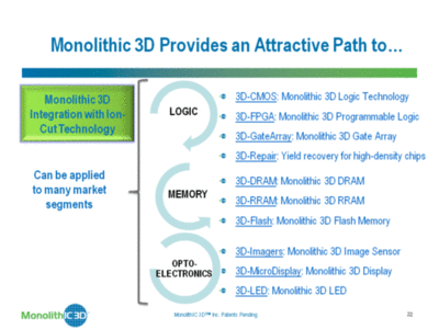
One application that monolithic 3D especially appeals to is the memory industry. Doubling memory capacity via traditional scaling is very expensive. Especially in manufacturing NAND flash, where traditional scaling results in smaller devices that can do less. Instead of making them smaller, they can be built one on top of the other, stacking layers together. In one lithography step multiple memory bits can be generated on multiple layers.
Or-Bach says memory makers such as Toshiba, Samsung, Hynix, and Micron are developing polysilicon-based monolithic 3D flash memories, but those transistors are not as effective as crystallized silicon. “Our technology allows memory to be built on crystallized silicon,” he said.
“In our industry, it’s not the cost of material that gives us the advantage; it’s the cost of manufacturing. If you can use the CAPEX to generate more memory base, you’re coming out ahead,” he explained. He says he believes MonolithIC 3D’s approach will be even cheaper than scaling because it uses the same equipment. As result, monolithic 3D is becoming real in the memory space, and is expected to reach production in the next year or two, notes Or-Bach.
Monolithic 3D can also be applied to logic devices. Or-Bach says just like with memory, there is a scaling advantage, and allows for generating a device equivalent in power, performance and cost as the next node, just by going vertical. “Every node comes with more pain and more risk,” says Or-Bach. “We believe that scaling to smaller dimensions is becoming harder and harder. Foundries would be at an advantage if they can build products using monolithic 3D at a lower cost. “
Aside from MonolithIC 3D, there are other players in the space. As previously mentioned, Toshiba, Samsung, Hynix and Micron are all developing their own versions. CEA Leti presented a paper on what they call 3D sequential integration at last year’s IEDM conference. Additionally, Oregon-based Besang has developed a version of the technology.
Integrating 3D TSVs and Monolithic 3D
On a final note, it’s important to note that 3D TSV technology and monolithic 3D are not necessarily mutually exclusive. Ultimately, these technologies can be integrated to produce the ultimate 3D system. “The beauty of monolithic 3D, is once one has the device, you can use normal 3D processes to connect those devices, to create heterogeneous structures integrating memory, logic, etc.” At MonolithIC 3D, target applications include memory, logic and 3D electro-optics. Here’s a more detailed list of specific applications monolithic 3D is suited to.

I hope this clears up your lingering questions on what exactly monolithic 3D is all about. It certainly did for me. Special thanks to Zvi Or-Bach. I’m glad we had this little chat. ~ F.v.T.


