Is advanced packaging production coming back to the USA? The Navy (i.e. NSWC Crane) is currently seeking proposals from the industry for the development of technical and business plans to establish a secure on-shore design, assembly, and test capability. This facility should support the heterogeneous integration of state-of-the-art (SOTA) commercial integrated circuits (ICs) with defense specific application-specific integrated circuits (ASIC) and Department of Defense (DoD) specific applications leveraging integrated Radio Frequency (RF) and sensor technology. The design centers will be referred to as the Secure SOTA Heterogeneous Integrated Packaging Prototype Design Center (SHIP-DC) while the manufacturing capability will be referred to as the Secure SOTA Heterogeneous Integrated Packaging Prototype Assembly and Test Center (SHIP-ATC).
As explained by program manager Brett Hamilton, “…the high-level objective of this program is to provide our warfighters reliable state-of-the-art microelectronics….we need to combine the best of state of the art, but also allow the DoD and the primes to customize that by creating a “heterogeneous integrated packaging solution that is a combination of DoD-unique die with the latest and greatest SOTA die.”
A Plan for Onshore Advanced Packaging Production
In terms of access, the plan is to come up with an advanced packaging production solution that is accessible to the entire industrial base giving us the ability to more rapidly integrate technologies to modernize our systems.
Hamilton made clear that this is not an R&D program: “The intent of this program is to transition the best in commercial practices into a secure facility where DoD and DoD primes have access.” This should be a commercially owned and operated facility with a self-sustaining business model that is made accessible to:
- DoD/US Government
- Defense industrial base
- Academia for test chips and research
- Commercial companies – to make the business case self-sustaining
The facility should be compliant with International Traffic in Arms Regulations (ITAR) and potentially up to secret-level design and manufacturing capability allowing secure assembly, personalization, and final test.
A Self-sustaining Solution
An important focus of this proposed program is for this business to ultimately be self-sustaining. A big part of the program’s Phase One effort will be not only to develop the technical plan but also the business plan, which should include an analysis of the industrial base, what their requirements are, and a roadmap to show that production is in place and can become self-sustaining. They will encourage non-DoD customers in order to get the production quantities up and help make the facility self-sustaining. There may be constraints on making parts for foreign companies.
Ultimately, for production, the facility will need to be a DMEA-accredited ITAR facility with the potential to do up to “secret” level design and manufacturing.
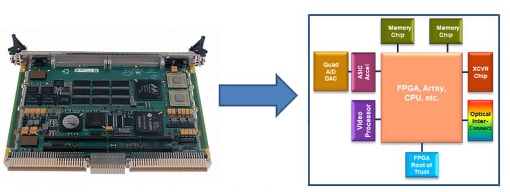
The slide below shows graphically what they are trying to accomplish. Basically, take what is currently on a circuit board and shrink it down into a heterogeneously integrated package. The SWAP benefits will be huge for military devices with power, size, and weight constraints.

This effort could include 3D-stacking, but 3D is not a requirement for this initial effort. The constraint in the initial program phase will be to “include the individual dielets (chiplets) integrated into the package in 2.5D fashion.” This will also allow mixing and matching technologies i.e CMOS and non-CMOS.
The holy grail for this technology would be to take a traditional TR module and shrink it down to a very small form factor that would enable it to be moved to the front end near the antenna system so data acquisition and signal processing can be performed right at the array. This very powerful solution is of great interest to the military.

Program Specifications
Teaming up to deliver complete solutions for both digital and RF has been suggested. The listed program specifications are described as general guidelines, and not hard-and-fast rules. In general, they are looking for the best technology available.
Design centers must be able to design RF and digital interposer and packaging interconnect for RF chips, not design the RF chips themselves. Designs must also adhere to the interface standards developed under the DARPA CHIPS program to ensure proper insertion and testability of the final product. Other details to consider:
- Diverse dies coming from different foundries/design teams must meet interface standards.
- There could be multiple proposals funded for Phase One of both digital and RF designs.
- As part of Phase Two, a package design kit (PDK) will be developed for future DoD customers.
The key stakeholders for this program are the defense/industrial base, the intelligence community (who will be represented on the source selection board), NASA, and anyone with high-performance electronics requirements. The prime provider must be a domestic company.
The program will be divided up into 4 phases as follows:
- Phase 1: Develop an Advanced Prototype Capability Plan
- describe engineering, mechanical, architectural, and other elements required to construct the SHIP-DC and SHIP-ATC.
- Phase 2: Advanced Prototype Capability Development and Initial Design Activities
- Phase 3: Install and Qualification of Processes
- Phase 4: Operate and Maintain Advanced Prototype Capability
Some of the specs that they are proposing to meet for the manufacturing facility are outlined in the following tables:


IFTLE will be following this program and will let you know when program participants have been chosen. For all the latest on advanced packaging, stay linked to IFTLE…………………………..


