


Commercial Times reports that TSMC’s Arizona wafer fab, Fab 21 Phase 1, has officially entered mass production on its 4nm process. Monthly capacity is expected to reach 30,000 wafers by mid-year.
Construction of Fab 21 Phase 2 and Phase 3 are set to proceed this year and next, with fab completion slated for 2025 and 2027, respectively. These expansions will gradually introduce the nanosheet transistor structure for TSMC’s 2nm process.
Super interesting to IFTE, the same report suggests that industry observers believe TSMC may add advanced packaging capacity in Texas, “…filling a critical gap in the chip manufacturing process”.
The report indicates that Apple plans to manufacture its A16 processors using the TSMC N4P process. AMD, will reportedly use TSMC’s 4nm on the production of its HPC chips, while NVIDIA reportedly plans to produce its B-series chips on the 4nm process as well, as per the report.
Apple and AMD are known to be current customers of the Arizona plant. According to Reuters, NVIDIA is reportedly in talks with TSMC to manufacture its Blackwell AI chips at the new Arizona fab as well.
Reuters notes that NVIDIA’s Blackwell chips, introduced in March of 2024, have, up to now, been exclusively produced by TSMC in Taiwan. Blackwell is highly sought after for generative AI and accelerated computing.
However, it is worth noting that though TSMC plans to handle the front-end production of NVIDIA’s Blackwell in Arizona, the chips need to be sent back to Taiwan for packaging, the Reuters report notes, for the Arizona plant lacks the chip-on-wafer-on-substrate (CoWoS) capability required for Blackwell.
That is an absolutely ridiculous situation and IFTLE is confident that that will be resolved in the short term. IFTLE has recently reported that TSMC has teamed up with Amkor US to soon offer advanced packaging and testing services for the Arizona plant.
It is likely that this Amkor collaboration will be the missing puzzle piece needed for the U.S. to establish a full domestic AI supply chain.
According to Commercial Times. AWS plans to use TSMC’s 3nm process to produce its latest AI chip, Trainium3. The cloud giant is reportedly interested in booking the capacity of TSMC’s second fab in the U.S.
Nvidia Demand
When asked in January whether Nvidia was cutting TSMC Blackwell CoWoS orders, CEO Jensen Huang said “As we move into Blackwell, we will use largely CoWoS-L. Of course, we’re still manufacturing Hopper [Nvidia’s GPU architecture platform before it announced Blackwell], and Hopper will use CowoS-S. We will also transition some CoWoS-S capacity to CoWos-L.”
Nvidia has been selling its Blackwell chips as quickly as TSMC can make them, but packaging has remained a bottleneck due to the aforementioned capacity constraints.
Let’s refresh our memories as to the structures of CoWoS S and L:
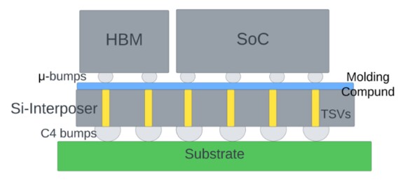
CoWoS-S: This technology uses a monolithic silicon interposer along with through silicon vias (TSVs) to facilitate direct transmission of high-speed electrical signals between the die and the substraten (Figure 1).
CoWoS-L: This uses local silicon interconnect (LSI) along with RDL interposer together forming a reconstituted interposer (RI). In addition to the RDL interposer, it also the preserves the attractive feature of CoWoS-S in the form of TSVs. This also mitigates the yield issues arising due to the use of large silicon interposer in CoWoS-S. In some implementations, it may also use through insulator vias (also known as through mold vias) instead of TSVs to minimize the insertion loss m (Figure 2).
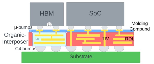
CoWoS-L is a chip-last assembly because the interposer is fabricated first and then followed by stacking of the wafer die on top. Once the interposer is fabricated, the next step is creation of the through insulated vias in the wafer die. The known good dies (KGDs) are then mounted over the wafer. The gaps between the die and the TIV are filled with molding compound, after with CMP process is employed to obtain a planar surface.
Next, two RDL layers are fabricated. The first on the interposer front-side to connect the wafer and the substrate via μ-bumps and the second RDL on the interposer back-side to connect the interposer and the substrate via C4 bumps.
For all the latest on Advanced Packaging stay linked to IFTLE……………………………..


