


Heterogenous integration and AI are currently moving forward hand-in-hand as the demand for greater computing power in theory, reduces the energy and time needed to train models; (although, DeepSeek may now change some of the thinking along these lines).
Larger more complex packages are being built to manage the learning process. Nvidia’s latest AI processor is a 2x reticle, and TSMC discussed its OIP a 9x reticle package using the A16 process and the CoWoS combined with the SoIC technology. The package will have 12 HBM4 modules for memory support. (Figure 1)
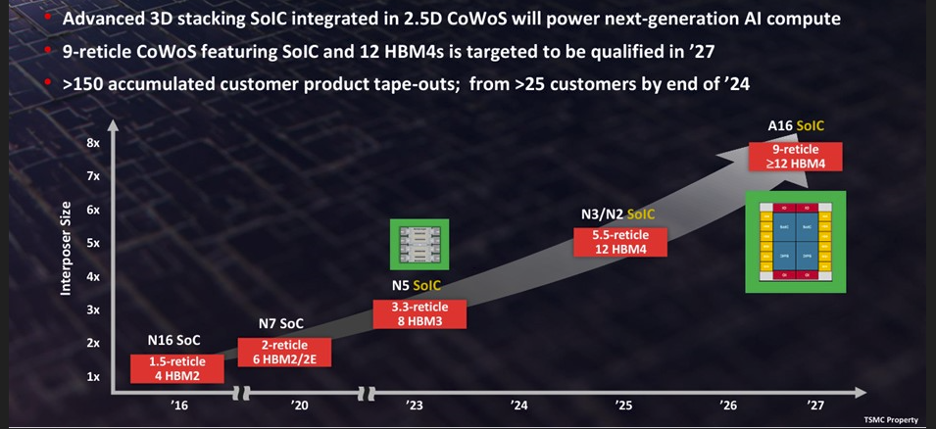
The expectation is that by 2030, these multi-reticle packages will reach the goal of 1 trillion transistors in a package, or at least that is what TSMC, Intel, AMD, and others mentioned at the SEMI ISS event in January of 2025. Packaging and how it would drive the industry and high-performance compute was a key element of this year’s ISS conference.
According to the presentation by TSMC’s Kevin Zhang, PhD, Senior VP, of Business Development and Global Sale, high-performance computing currently makes up 40% of the industry’s revenue. There is also a considerable focus on packaging technology as it drives the ability to place multiple dies and, more importantly, memory in the same package, which helps improve latency and reduce power consumption. Reducing power is critical from the current supply and demand outlook of how much power data centers will potentially consume, and latency is crucial as intelligence moves closer to the edge. 1 millisecond is a necessity in self-driving cars, not just nice to have.
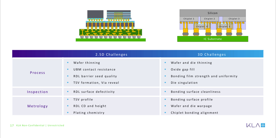
Oreste Donzella, Executive Vice President and Chief Strategy Officer, KLA, gave an excellent overview of the transition to advanced packaging, and the shift to heterogeneous integration. Donzella touched on the challenges of 2.5 and 3D packaging and how the processing brings front-end challenges to packaging with cleaning, metallization, and etching, not to mention defect detection.
To achieve these large multi-reticle packages, the speakers mentioned several technology changes that are taking place. The first is panel-level processing (PLP) which helps with throughput and yield, as more packages can be processed at the same time. They also talked about large interposers with embedded components and co-packaged optics.
Currently, redistribution layers (RDL) using photoresists are the process of choice, but solid interposers, as well as glass panels, are in development. Rahul Manepalli, PhD, Intel Fellow & Director of Substrate Packaging Technology Development discussed the motivation for moving to glass core substrates. Key areas such as dimensional stability over RDL, greater through-hole density which can improve bandwidth, and higher temperature stability can offer some processing benefits.
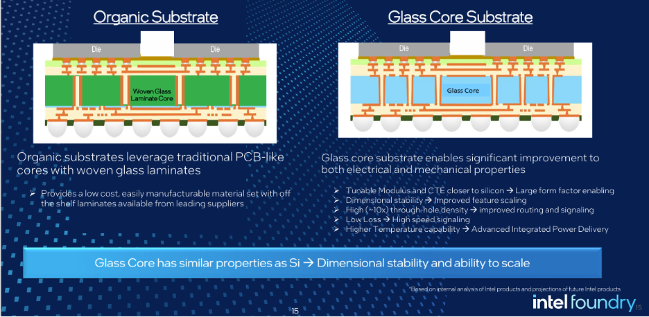
Manepalli went on to say that glass substrates can offer scaling advantages, with smaller lines and spaces and smaller bump scaling. You can also implement lower dielectric constant materials, and processing on glass gives cleaner copper lines. Not to mention that there is the possibility of placing more dice on glass substrates than using RDL and glass laminates.
Meeting the Limits of Scaling: Is Hybrid Bonding the Answer?
To continue scaling these massive packages the industry is moving towards hybrid bonding. Jan Vardaman, President of TechSearch International, moderated a panel on hybrid bonding. Panelists included Rajit Seahra, Senior Fellow, AMD; Manish Ranjan, Head of Business Management, Heterogeneous Integration, Applied Materials; Akshay Singh, PhD, VP, Advanced Packaging Technology Development, Micron Technology; Ming Zhang, PhD, VP, Fabless Solutions, PDF Solutions.
Jan had an excellent list of questions and then left time for audience participation. The advantage of hybrid bonding is that smaller pitches can be used, thus increasing the IO and the bandwidth communication between chips on the packages. For wafer-to-wafer bonding the panelists discussed 50nm pitches, which would result in smaller packages. With hybrid bonding, the power and heat issues would be improved due to better contact resistance and increase IO’s.
The panel discussed the potential for higher reliability as the hybrid bonding would eliminate any cracking of bumps, and it also reduces the contact resistance between chips. High-bandwidth memory is a good candidate for hybrid bonding and there is a great deal of work taking place on the process according to the panelists, but they were non-committal to when hybrid bonding might be implemented.
This was a bit surprising as it has been presented on roadmaps as being ready at HBM 4, but only time will tell. There are the challenges of die-to-wafer, and wafer-to-wafer contact, cleanliness, planarization, and other process challenges that were discussed by the panelists.
Companies that are vertically integrated will implement hybrid bonding first; however, there are still many challenges with equipment and material infrastructure to be overcome. Cost is a consideration, but the consensus was that if you used intelligent design and process it would likely result in lower cost.
The drive to multi-reticle packages for HPC is moving forward rapidly. The conference highlight both the successes and future challenges for advanced packaging for HPC. Vertically integrated companies are making great strides in moving the technology forward, there are slight differences in the roadmaps, but isn’t that what technology and competition are all about?


