


I have spent a considerable amount of time covering the technology associated with the front-, and back end of-the-line. So for me, it is remarkable to see the growth in advanced packaging and how the interest in packaging technology seems to be overshadowing the FEOL transition to gate all around transistors, and to a certain extent backside power.
This transition was evident at the recent TSMC North America Open Innovation Platform (OIP) Ecosystem Forum held in September in Santa Clara. TSMC holds this event each year to acknowledge its partners and demonstrate its technology and roadmaps to the industry. The foundry ecosystem doesn’t happen without its partners.
For those of you who have been around long enough, the OIP started out as the Grand Alliance and has continued to add partners, as well as customers. One of the reasons for TSMC’s foundry dominance has been their ability to create, and then manage the OIP as a well-oiled machine. Many of their customers find the movement from design to tape-out to silicon to packaged product to be seamless.
While the FEOL part of the OIP has operated for many years, with the transition to 3D packaging and chiplets, the packaging part is a growing entity. It was a key focus at this OIP, according to a recent blog by Dan Kochpatcharin, Head of Ecosystem and Alliance Management Division, TSMC.
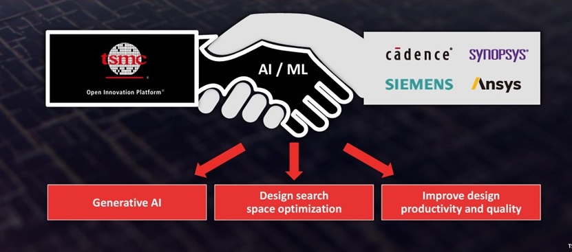
The TSMC OIP ecosystem fosters collaborative design with partners and customers to advance 3D architectures for the chiplets of the future. One of the challenges with 3D packaging is optimizing design, layout, ease of manufacturing, and the resulting power, performance, and area (PPA) that drives the microelectronics industry. By leveraging its participation in the 3DBlox standards organization, TSMC’s OIP is creating designs and packaging using TSMC’s 3DFabric’s for advanced packages. These include TSMC’s Integrated Fan-Out wafer level packaging (InFO), System on Integrated Circuit (SoIC), and Chip on Wafer on Substrate (CoWoS) technologies.
TSMC had already announced its intentions to move to substrate technology in a big way. The company recently purchased a 5.5G flat panel factory. In the press release, they commented that they plan to use at least 50% of the process equipment in the fab.
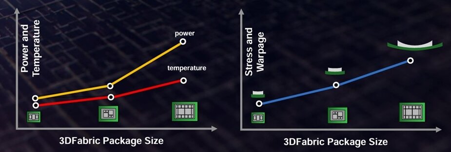
The challenges of moving to panel-level packaging were outlined in the OIP presentation (Figure 2). These include -power and temperature, stress, and warpage due to the larger panel size. This is where the EDA simulation tools for 3D packaging can help with modeling the thermal analysis, and the mechanical stress. Design Technology Optimization (DTCO) will be as important, if not more important for 3D integration as it is for the FEOL transistor and metallization design.
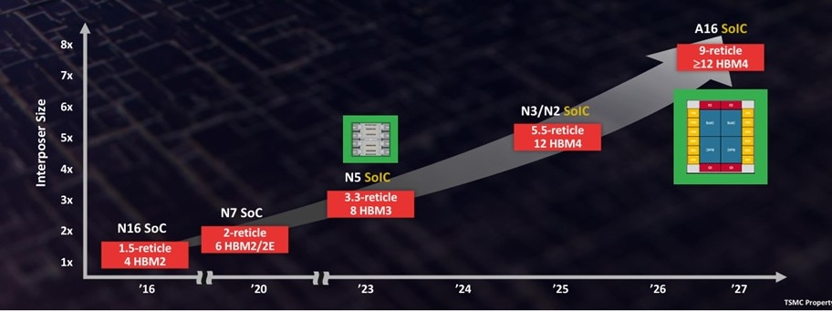
As it does so well, TSMC laid out the roadmap for advanced packaging. Recently TSMC and Nvidia made news with a 2-reticle package for AI technology. TSMC using its SoIC process at the N5 technology offers a 3.3 reticle package using eight HBM 3 memory stacks. In 2025 a SoIC 5-reticle package at the N3/N2 technology nodes will be released into production using 12 HBM4 stacked memory. In 2027 at the A16 technology node TSMC will be manufacturing a 9-reticle package with greater than a 12 HBM4 memory stack. This is an aggressive roadmap moving forward. It will be interesting to see how big the substrate is for a 9-reticle package. Since a 5.5G panel is ~ 1200×1200 mm it looks like TSMC is planning for the future (Figure 3).
Currently, TSMC is the foundry of choice for advanced technology and advanced packaging. While there is competition at process technology nodes and advanced packaging, TSMC still maintains a significant market share advantage. As 3D packaging emerges into the mainstream it remains to be seen if the competitors can up their game and take market share away from TSMC. To do so they will need to build a partner ecosystem as strong, and reliable as TSMC.


