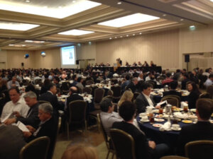
The 65th annual Electronics Technology Components Conference (ECTC 2015) logged record numbers (over 1500 attendees, 20% increase over last year) as the entire semiconductor industry recognizes (finally) that there is indeed money to be made in the advanced packaging sector.
The flip chip and wafer level packaging sessions were full to overflowing. The 3D tech sessions offered lots of fresh content and innovative presentations and were also well attended. This was good sign after it appeared there was a lull in 3D integration progress for the past year as the industry waits for a sign from someone or some thing that 3D really is happening in sufficient volumes to make all the efforts worthwhile. According to John Lau, ASM, that sign will be from Intel when they announce shipment of Knights Landing with stacked DRAM from Micron inside.
3D topics were conspicuously absent from the plenary and special sessions, which is as it should be, as we’ve taken 3D past the hype and are implementing it now in real manufacturing situations. It’s been replaced by the latest trends such as sustainability in microelectronics, the Internet of Things (IoT), packaging for bio-medical technologies, nano-packaging, and liquid cooling for high performance systems. Interestingly enough, 3D integration technologies can enable most of these trends, whether its at the device level or system level. For example, last year the 3D InCites Award for the Device Category went to Sorin CRM for its 3D IC module for medical implant.
The real 3D story came from the buzz in the Technology Corner, where a number of suppliers could see a marked difference between this year and last year in the interest level for products serving 3D technologies. According to Gene Jakobowski, E-System Design, there’s much more talk and activity about 3D programs. “We’ve talked to some pretty high profile customers who are starting 3D programs in the next few weeks,” he said, adding that they are Tier 1 customers, but couldn’t disclose exactly who.
“Guys who were on the fence are starting projects,” noted Bill Martin, E-Systems Design. “They’re complaining about the cost, but generally when they’re focused on cost, it means they’re more serious than they were.” He also noted that they are beginning to understand that while the device cost might be high, the system cost built using 3D integration technologies is reduced.
“People are now busy producing 3D and talking less about it – and complaining less about temporary bond/debond issues,” noted Paul Lindner, EV Group. For years, he said tool sales went to outfit pilot lines, but now more systems are heading to adding capacity. “For us, there’s no doubt that the investment in 3D TSVs has paid off.” Should we be concerned about alternatives continuing to push out 3D commercialization? Lindner says, “No, because the alternatives don’t deliver on the promise of 3D being, faster, lower power, and reliable. DRAM in a data center has to be very robust. Alternatives also need time to mature.”
While many have complained about how long it’s taken for 3D to take off, Laura Mauer, Veeco Precision Surface Processing, sees a silver lining. Veeco has developed wet etch processes for TSV reveal, which the company claims offers a lower cost alternative to plasma etch for this step. Mauer says that because of the delays of 3D TSV going in to HVM, companies who have invested in development of processes are now looking at alternatives that will improve cost and yield. “The delays have allowed for the time to look around at what else is out there and its given us time to develop and improve processes, along with our chemical partners,” she said, adding that she is seeing a lot of interest. “We’re doing big demos for big companies for TSV reveal, resist strip, and UBM etch,” she said.
Admittedly, there are companies still waiting for the investment in 3D to pay off. “It’s a long developments cycle for anything new, and it’s going to be a while before we see payback. People are still looking for temporary bond and permanent bond solutions,” said Ken Seifert, Dow Corning. Andrew Ho, also of Dow Corning, says, with regard to 3D in HVM, it’s there, but cost is still an issue. “Alternative solutions are also being developed, that’s a major hurdle to vast adoption of TSV. It requires a collaborative effort to drive the cost down.” Two years ago, Dow Corning introduced its temporary bond/debond solution at ECTC 2013. Last year, Ho introduced the concept for a thermal interface material in development for flip chip applications that would also be suited for 3D IC assembly. This year, Ho reports that the technology has been validated by partners and will be implemented in high-end computing applications.
Then there are the rumors. While some at TSMC say that InFO is expected to be solution for pretty much everything, others say 3D is really taking off there. Want proof that 3D has been a worthwhile investment? I’m told its the biggest thing IBM is bringing to the party at GLOBALFOUNDRIES.
Many people I spoke to talked about the cycles new technologies go through. In general, the hype goes away because once something becomes normal business, people don’t want to talk about it. Once volumes start to grow, its news again. We saw it with flip chip and fan-out wafer level packaging. And we are seeing it with 3D. We just had to be patient. ~ F.v.T


