One of the ways I learn about advanced packaging technology and what it entails is by visiting our community member companies. There’s nothing like talking to the experts face-to-face and walking through a cleanroom or advanced packaging applications lab to drive home a concept.
For the past year, I’ve been talking with Bob Patti, Founder and CEO of NHanced Semiconductors, about the company’s growth and expansion in North Carolina and Indiana and the launch of a new business model he calls Foundry 2.0. Recently, Patti invited me to the Morrisville, North Carolina facility to get a first-hand look at Foundry 2.0 in action.
Who is NHanced Semiconductors?
Coming up on its 9th anniversary, NHanced Semiconductors spun out of Tezzaron Semiconductor in 2016 to focus on the high-end advanced packaging technologies that Patti and his team of design and packaging engineers first developed at Tezzaron. The team pioneered layer transfer stacking for DRAM memory.
Patti is a serial entrepreneur – having founded nine start-ups, including Tezzaron and NHanced. While he hails from chip design, he says his experience over the years has shaped him into an advanced packaging process engineer. He likes to say that NHanced specializes in leading-edge technology from 25 years ago.
So what does he mean by that? It’s simple: the company implements 25-year-old fab technology that is leading-edge for advanced packaging today. Advanced packaging isn’t done at the nanometer scale, he explains, so using advanced node processes and processing equipment for 2.5D interposer fabrication and 3D IC stacking is overkill.
“Moore’s law is dead, in terms of cost,” Patti says. “We can continue scaling but it’s expensive. Advanced packaging allows us to eliminate unused elements and reduce the transistor count, which directly reduces cost and power, and still meets or exceeds the needed performance.” He’s talking about the processes and technologies that will enable next-generation chiplet architectures, as well as complex systems-in-package (SiP) for specialty applications.
“All advanced packaging really boils down to is getting rid of the wire,” says Patti.
What Is Foundry 2.0 and Why Do We Need It?
Foundry 2.0 sources dies and chiplets from traditional foundries and applies semiconductor foundry processes and advanced packaging and assembly technologies. It uses front-end processes such as photolithography, chemical mechanical polishing (CMP), deep reactive ion etching (DRIE), and hybrid bonding processes. The results are highly interconnected 2.5D interposer assemblies, 3D stacked ICs, and chiplet configurations.
What makes Foundry 2.0 different from Foundry 1.0? Patti explained that while traditional foundries and IDMs are implementing 2.5D and 3D advanced packaging for chiplet integration internally, they can’t serve customers who want to tap into these technologies to integrate third-party chips – memory, for example – into the package. They also aren’t interested in customization or low-volume applications.
“Foundry 1.0 operates on the theory: You can get any color you want, as long as it’s black,” says Patti, as an analogy. At NHanced, you actually can get any color you want. And because NHanced doesn’t make transistors, its not competing with its customers. The company partners with all the leading-edge foundries to source their chips, then adds its own magic to turn the chips into custom devices.
Another key differentiator between Foundry 2.0 and Foundry 1.0 is reduced manufacturing cost. By using legacy tools and processes for the basics and reserving the leading edge for the “special sauce,” he’s able to keep the cost down lower than what the tier-one foundries and IDMs can do.
The timing couldn’t be better for NHanced and Foundry 2.0. The semiconductor industry is changing, driven by the needs of artificial intelligence (AI) and other high-performance computing applications. Rather than being volume-driven, it’s now value-driven.
“The profit margins for fabs and IDMs are taking a hit, and the end users like NVIDIA are seeing the profits. If we continue to rely exclusively on Foundry 1.0, the costs of semiconductor devices will continue to increase, and so will the cost of our end devices,” says Patti.
The Birthplace of Hybrid Bonding
The facility in Morrisville, North Carolina, where I visited, is also the birthplace of hybrid bonding. It was invented in this building by Ziptronix (now Adeia) by Gill Fountain and Paul Enquist. Fountain still shares office space with the team. NHanced bought the building in 2017, along with a full technology transfer license from Adeia, and is now the first company to implement hybrid bonding in its processes for heterogeneous materials like silicon and glass, and silicon carbide.
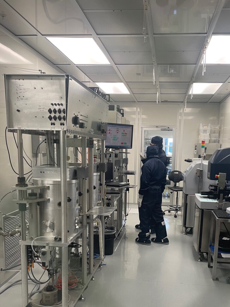
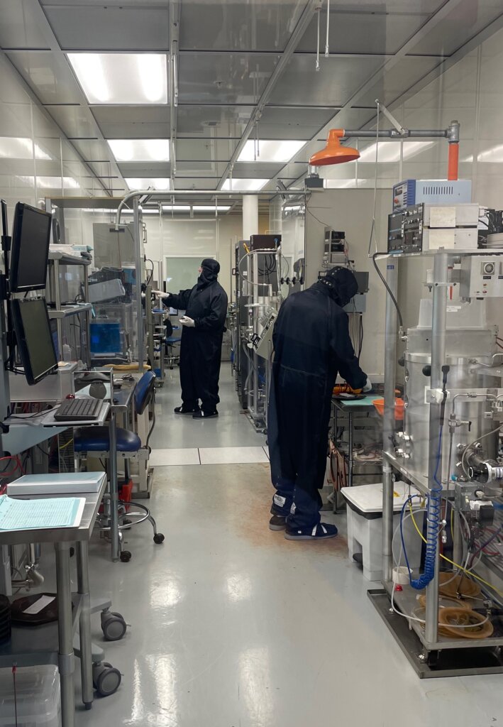
The cleanroom space is outfitted with mostly refurbished equipment; workhorses that excel in performing legacy node processes that are well suited to the feature sizes for the most advanced packaging processes.
But when a process calls for a new, leading-edge tool, Patti happily invests in it. For example, the company recently bought one of the very first Besi Datacon 8800 CHAMEO systems for room-temperature direct fusion and hybrid bonding processes.
Patti says the company does virtually all the advanced packaging for the federal government that requires hybrid bonding.
“The good news is we’re drowning in business,” says Patti. “For hybrid bonding, our facility will be able to produce larger volumes than TSMC by 2026.”
Expansion Plans for NHanced
NHanced is 100% self-funded. There are no investors and no debt. And while NHanced was in the running for CHIPS Act Funding, Patti believes they were passed over primarily because the model he proposed targeted lower volume production rather than typical OSAT high volume manufacturing.
But this hasn’t stopped Patti’s plans for expansion. Up until now, NHanced has been primarily a development company but is now ramping up to become a volume manufacturer of high-mix devices. Patti anticipates that the company, which has seen 10x growth in the last two years, will see another 10x increase in revenue over the next five years. Growth plans are in motion. Patti’s excited to partner with governments in Indiana and North Carolina to implement those plans, along with local researchers like the Applied Research Institute and academia including North Carolina State University, Ivy Tech, and Purdue University.
Headquartered in Illinois, in 2023 NHanced invested in a volume production advanced packaging facility in Odon, Indiana. The ribbon cutting was in January, and at this writing the building and cleanrooms are complete. According to Patti, the gas lines are being installed in the fab, and half the equipment has been installed.
While he was originally eyeballing a second Indiana manufacturing site to further implement Foundry 2.0, he has now pivoted to focus on expanding the existing North Carolina location. The site currently produces 250 wafers per month (wpm) – but orders are exceeding capacity. So they are adding a second shift, expanding the cleanroom footprint, and installing automated 200mm and 300mm tool lines to accommodate volume production.
Between the two locations, Patti expects an output of 15,000wpm.
Expansion plans in Indiana and North Carolina are expected to bring high-paying jobs to the regions. Realizing that technician jobs in an advanced packaging foundry are specialized, Patti says they offer extensive training and above-average pay. “These investments provide long-term return because employees tend to stick around,” he says.
What the Future Holds for Foundry 2.0
Patti predicts a paradigm shift for the semiconductor industry. He envisions a future where microelectronic devices are more customized and transistors are fewer but more powerful. He hopes that Foundry 2.0 is a concept that other companies adopt. Patti hasn’t patented the phrase. He’s just setting the example for other players in the industry. It’s time for all companies like NHanced, which excel in customization, to thrive.
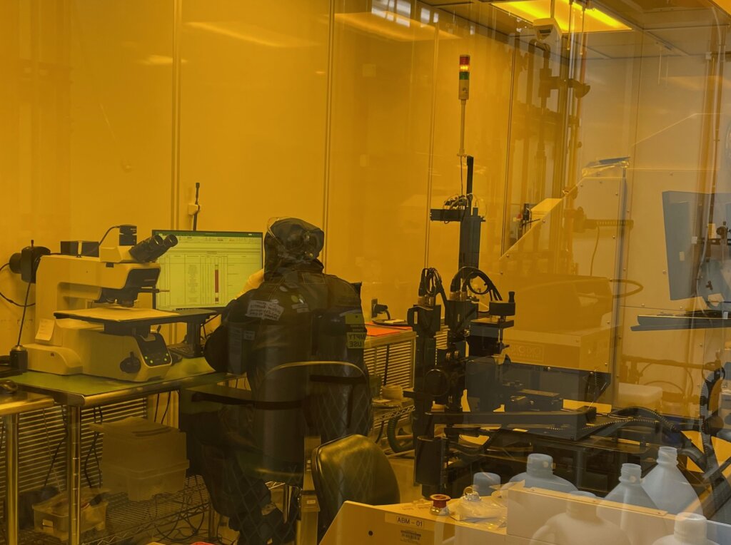
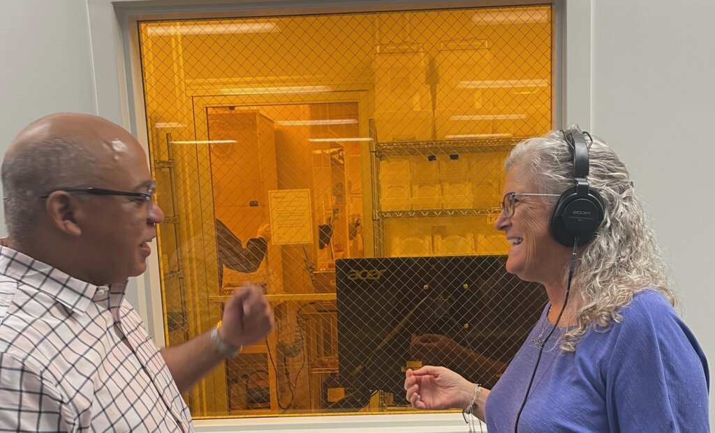
To hear Patti describe Foundry 2.0 in his own words, listen to the podcast. We also take an audio tour of NHanced’s North Carolina cleanrooms, guided by operations director Carl Petteway. Photos of the window tour showcase the class 100 and class 1000 cleanrooms, and the lithography cleanroom.