In IFTLE 626 we looked at the Yole article that addressed the question of whether panel level processing was finally coming on line. In this blog we will take a look at some of the work Amkor is doing on what they are calling hybrid panel level technology.
But before we do, I just wanted to remind the younger generation readership out there that this is not a new concept. In the mid 1990s my electronics division in Dow Chemical and Micro Module Systems (a spin out of DEC) won a contract (“Large Area Processing”) from DARPA.
Over a period of three years we installed a line in Cupertino CA and studied several options for scaling up this technology. In 1997 we actually made the cover of IMAPS “Advancing Microelectronics” magazine (see below…that’s me top row 3 from the right…). Not quite the cover of “Rolling Stone” but fun at the time none-the-less.
In the end, we couldn’t get the yield up high enough to make this a viable economic process. Now we find ourselves 25+ years later with better equipment and new concepts about how to make such technology work.

Amkor Hybrid Panel Level Package Technology (HPLT)
Amkor author Eoin O’Toole notes that the known technical challenges with panel-level fan-out (PLFO) packaging range from die-shift over the full panel, through warpage of the panel along the process flow, which limits the number of redistribution layers, to controlling the total thickness variation (TTV) during the panel-level back-grind processes. Commercial aspects such as capital expenditures on panel-level equipment and difficulty in filling a panel line are the main financial considerations.

Figure 1: Process flows for WLCSP and die-first fan-out. (Source: Amkor Technology)
The Amkor Hybrid Panel Level Package Technology (HPLT) is based on 650 x 650mm glass panels. This panel format permits the processing of either four 300 mm wafers / square panels, nine 200 mm wafers or 16 150 mm wafers.
To overcome the concern of filling a panel line, Amkor developed HPLT, which can be used in a wide range of package technologies including :
- Wafer Level Chip Scale Package (WLCSP)
- Wafer Level Fan-Out (WLFO)
- System-in-Package (SiP)
The process flow after assembly on the glass panel is effectively the same for WLCSP, die first WLFO wafers, or for panel-level fan-out (PLFO) panels. Descriptions for WLCSP and WLFO process flows are shown in figure 1.
The wafer or sub-panel is assembled on a large-format glass panel by means of a temporary bonding adhesive. The RDL layers are built up directly on the glass panel, starting with the under-bump metallization layer (UBM) and proceeding from the top RDL layer to the bottom RDL layer with the respective interlayer dielectrics. After completion of the bottom RDL layer, an additional UBM layer is required to enable flip-chip assembly of the die onto the RDL stack.

Exposure is performed on panel-level stepper equipment with the alignment performed on an individual wafer or sub-panel basis. The developer process is performed once again on a panel-by-panel basis. The bill of materials (BOM) was selected to provide identical mechanical and chemical characteristics of redistribution layers processed on the wafer process line. For the die-last, or RDL-first, application of this technology, the process flow is inverted, as shown in figure 3.

Subsequent to the flip-chip assembly, a mold underfill (MUF) process or, for finer pitch applications, a capillary underfill (CUF) and mold process can be used to complete the encapsulation of the device. The glass panel can then be debonded from the molded device.
Currently available flip-chip and mold equipment require that the glass panel must be subdivided into smaller dimensions, which means that the glass panel cannot be reused in this application. This limitation may be overcome by using panel-level flip-chip and molding.

Amkor’s HPLT focuses on the most expensive element which are the RDLs themselves. The process steps which will have a significant cost benefit of massively parallel processing are performed on a panel basis. This includes coating and developing of dielectric and photo resist layers, exposure of the dielectric layers and photo resist layers, curing of the dielectric layers, physical vapor deposition of the seed layers, electrochemical deposition, photo resist strip and chemical wet etch of the remaining seed layer. A six-metal layer RDL-first test vehicle (TV) was fabricated as shown in Figure 6.
Reliability
Singulated units were subjected to a series of reliability testing. The focus of this reliability assessment was to determine both layer adhesion and package integrity. Results of the reliability tests performed are shown in the table below. All results were positive with no fails observed after stress tests.
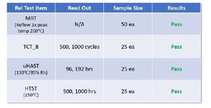
They conclude that “Based on the results to date, further studies are encouraged to fully explore the manufacturability and reliability of this packaging technology.”
For all the latest of Advanced Packaging stay linked to IFTLE…………………………………….