


By Till Dreier & Julius Hållstedt, Excillum
In 2025, it is now clear to those who manufacture semiconductor devices that the path to enhanced performance, lower power consumption and lower cost per function lies in chiplet integration using advanced packaging technologies. However, as package feature sizes shrink and interconnect densities grow, ensuring manufacturing quality and reliability has become more challenging than ever. Efficient fault isolation, failure analysis, yield improvement and quality control all rely heavily on advanced characterization and metrology tools—where X-ray imaging plays a crucial role. From early-stage process development to high-volume production (lab to fab), X-ray inspection provides the 3D visualization and capability for non-destructive insights needed to evaluate hidden structures, identify defects, and optimize manufacturing processes.
This article provides the background on the key design considerations necessary to maximize the potential of 3D X-ray methods for electronics R&D and manufacturing. It outlines the fundamental principles of X-ray imaging, explores critical factors influencing measurement performance, and discusses best practices for optimizing setups based on geometric magnification. By understanding these factors, engineers and researchers can unlock the full capabilities of X-ray technology.
Understanding resolution
When talking about resolution, there are several parameters that actually matter. Let us begin by defining resolution and examining its practical application.
The achievable spatial resolution in an image is defined as the ability to distinguish two closely spaced features. This is affected by many parameters of the imaging system, which we will discuss in the next section, but will finally be limited by the diffraction limit (Figure 1).
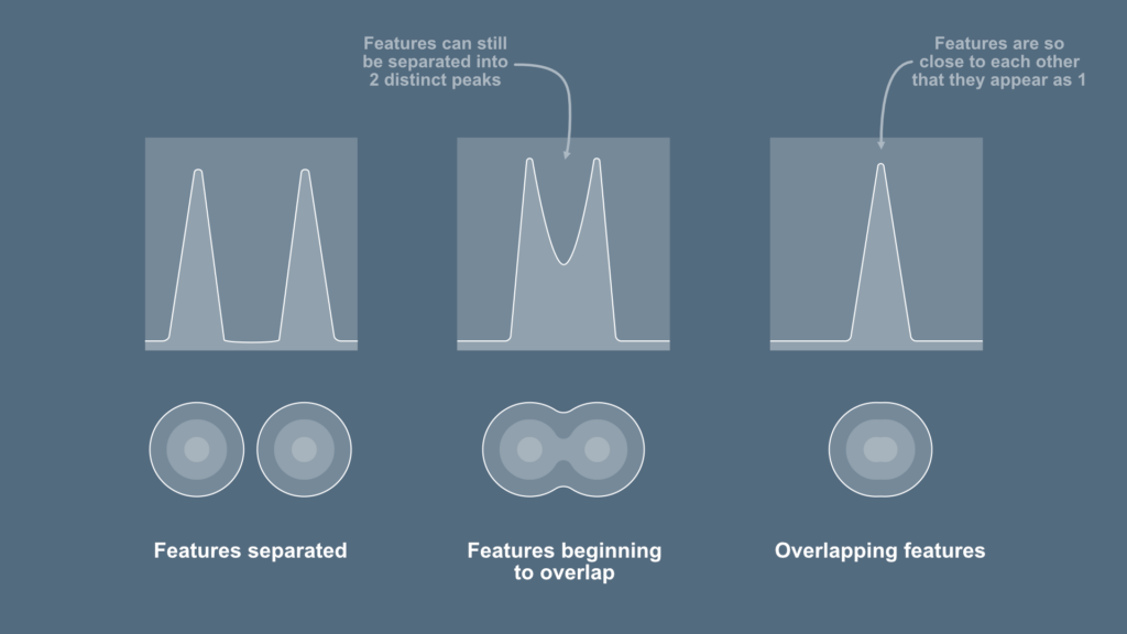
A common way to assess resolution is the Modulation Transfer Function (MTF), which describes how well an imaging system can capture details of different sizes. It essentially shows how much fine detail is preserved in the final image, helping to quantify the sharpness and clarity. In practical terms, the resolution can be measured using resolution charts such as JIMA, siemens stars or similar, these are third party reference samples consisting of repeating lines and spaces at different distances. The finest spacing that can be resolved is then defined as the achievable instrument resolution.
Besides the resolution definition as describe above, other terms are sometimes used that may be misinterpreted as resolution. The first example would be defect detectability or feature detection limit. This is the smallest feature that can be seen in an image and depends on contrast and noise. For instance, a dense particle in a soft material may be visible even if it is smaller than the system’s resolution limit, since it stands out from its surroundings, while a low-density particle in a soft material may stay hidden.
The second example is the effective pixel size and the voxel size, describing the smallest units into which a 2D image or 3D volume is divided. Smaller pixels/voxels are achieved by increasing the magnification, allowing to capture finer details. However, they are not equivalent to the spatial resolution but define the lower resolution limit in the specific image. The achievable resolution depends on the X-ray focal spot size, detector sharpness, and system stability.
Key factors affecting resolution and image quality in X-ray CT
Having discussed resolution, let us now examine strategies to enhance resolution in X-ray imaging and computed tomography (CT) applications. We will identify the relevant parameters that must be considered in achieving optimal resolution.
Geometry
Using geometric magnification, high resolution is achieved by maximizing the magnification , which is the ratio between source-detector distance (SDD) and source-object distance (SOD) as shown in Figure 2. The achievable effective pixel size peff depends on the physical pixel size p of the detector, and M.
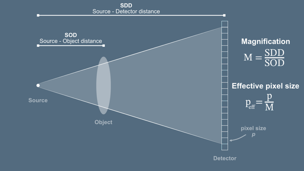
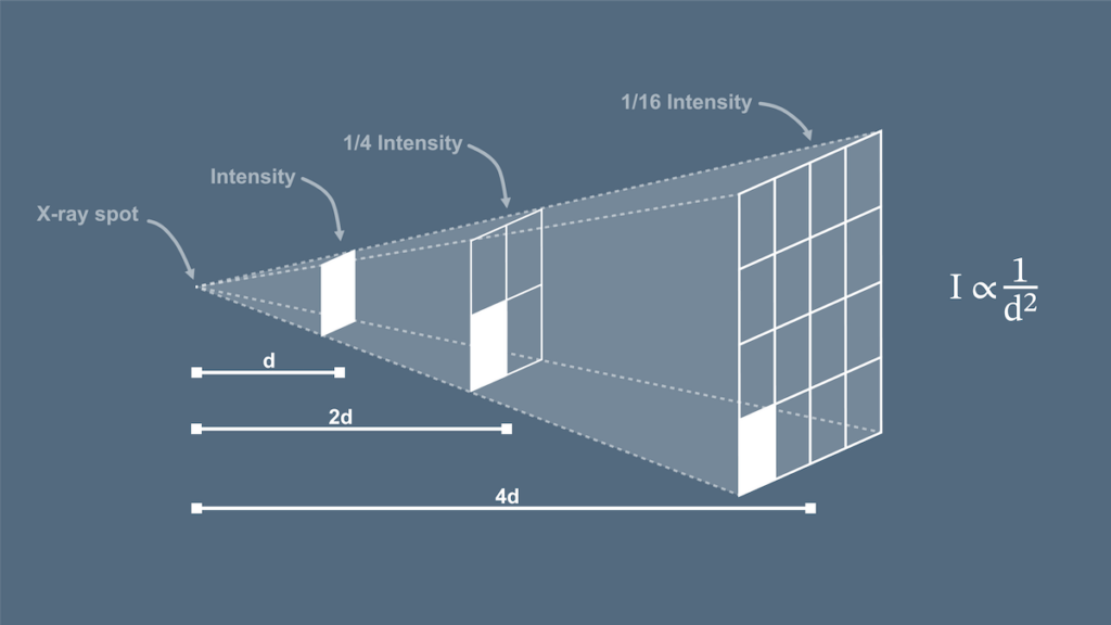
There is a trade-off: the inverse square law (Figure 3). As the distance from the X-ray source increases, the emitted X-rays spread out reducing the intensity per area by the distance squared. This means, that doubling the distance will reduce the intensity by a factor of 4. To achieve short scan times, SOD should be minimized to have as many photons as possible on the object and SDD should be selected as short as possible to achieve the desired peff.
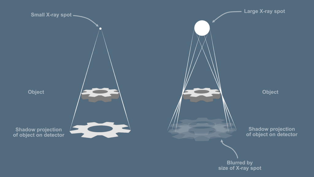
A key factor limiting the achievable spatial resolution is the focal spot size. If the spot is too large, the image will appear blurry (Figure 4). A simple rule of thumb is that the achievable resolution is approximately half the full width at half maximum (FWHM) of the focal spot size, considering a Gaussian-like spot profile. Smaller focal spots provide sharper images, enabling to see finer details.
The visible part of the object in the scan is described by the field-of-view (FOV), which is defined by the size of the detector and the magnification. Zooming in more, i.e. increasing magnification, reduces the FOV. Hence, achieving high resolution in a large object requires either a large detector or multiple scans. Additionally, it might be difficult to achieve a sufficiently small SOD with larger objects, leading to an increased SDD to maintain magnification and consequently longer scan times.
Balancing geometric magnification, field-of-view and X-ray intensity are key to achieve high resolution while keeping the scan time and noise at a reasonable level.
Equipment
To achieve high resolution and good image quality depends on the performance of all components involved: the X-ray source, the detector, and the mechanical components. While an imaging system might perform well for 2D imaging, e.g. as typically shown by imaging resolution gauges such as JIMA charts, achieving the same resolution in CT can become quite difficult since all used components are affected by changes in the environment. The behavior of X-ray sources and detectors also may change over time.
Practical considerations to optimize resolution and image quality in CT
Having discussed the factors influencing resolution and image quality, we will now explore practical strategies to achieve the optimal resolution and image quality in real-world scenarios.

Geometry
To maximize the number of photons on the object and detector, SOD and SDD should be as short as possible. The most crucial is minimizing SOD. A shorter SOD maximizes the photons per area on the object and allows for SDD reduction.
The object size can become limiting when the aim is to place the object a few mm or less from the source. Additionally, there is a trade-off between FOV and resolution. Increasing magnification will increase resolution and reduce the FOV, i.e. high-resolution in a large area can be difficult to achieve.
Setup mechanics
Stability is key to enable high resolution and long measurements. Vibration isolation, e.g. using air dampening, is almost always required to achieve sub-micron resolution. For highest stability, granite can be used instead of optical tables.
Additionally, thermal stability needs to be considered. Depending on the environment the system is placed in, active temperature control may be required. The material of the used equipment, e.g. linear stages and mounting brackets should be considered. Aluminium parts have significantly higher thermal expansion than e.g. stainless steel.
During a CT scan, the only moving part is the rotation stage. Important parameters to consider are repeatability, precision of motion, sphere of confusion, and wobble. High quality ball-bearing or air-bearing stages should be selected.
X-ray imaging detector selection
To select an appropriate x-ray imaging detector, the specific application should be considered. The scintillator/sensor material and thickness should be selected depending on the energy range that is useful for the specific application. If space is limited, smaller pixels might be preferable. However, larger pixels will collect more signal improving SNR. The PSF of the detector needs to be considered to meet the resolution requirement. The detector pixel matrix size should be matched to the required FOV and resolution needed.
The most common detector nowadays in both Medical and Industrial applications is what is typically referred to as FlatPanels. These consist of an X-ray scintillator material converting X-ray into light that is subsequently detected by a pixelated sensor chip. FlatPanels often have a PSF of around 2 – 3 pixels in horizontal and vertical direction.
When imaging lower density objects or requiring high detector resolution, CMOS cameras with small pixels can be an option. However, such detectors have much lower sensitivity compared to a FlatPanel. Challenging applications requiring very high speeds, high SNR, or when scanning objects with a wide variety of densities, photon counting detectors can be an option. These detectors process incoming photons individually, enabling noise-free readout, energy discrimination, and have a smaller PSF leading to sharper images.
Source optimization for X-ray imaging
When selecting an X-ray source for x-ray imaging tools, the key parameters are the spot size (including the stability of spot size and position), the acceleration voltage range, and the possible emission power at the desired settings. The spot size should be selected as large as possible to still be able to achieve the desired resolution while maximizing emission power, which reduces scan time and/or improves SNR.
To maximize performance in CT applications, the emitted spectrum can be tuned by adjusting the acceleration voltage. This will define the upper limit of energies emitted. Furthermore, by adding filtering (metal foils) to remove lower energy photons from the spectrum. These increase absorbed dose in the sample while not contributing to the measurement and may also cause artifacts when scanning denser samples.
Take aways
X-ray methods are essential in advanced packaging for a wide range of applications, from failure analysis to quality assurance, but performance is often limited by resolution, contrast, and throughput. In this article, we have explored how simple design and measurement geometry consideration impact 3D X-ray imaging, enabling improved defect detection, analysis and process control. By optimizing the X-ray source, detector selection, and sample position, the full potential of X-ray inspection can be unlocked.
Further reading:
- Dreier, D. Nilsson, J. Hållstedt: ”Fast and high-resolution X-ray nano tomography for failure analysis in advanced packaging“, Microelectronics Reliability 168 (2025). doi: 10.1016/j.microrel.2025.115694
- Dreier et al.: “Laboratory x-ray nano-computed tomography for biomedical research”, Journal of Instrumentation 19 (2024). doi: 10.1088/1748-0221/19/10/P10021
- Hållstedt: “Brightness as key performance metric for X-ray tubes and benchtop X-ray sources”, Excillum AB (2024).


