


By Bastian Troeger, Director Product Marketing & Sales Support; Eyal Segev, Director of Marketing
As artificial intelligence continues to push the boundaries of computing, the demand for high-performance processors has led to significant advancements in semiconductor design. The industry is transitioning from monolithic dies to chiplet-based architectures, integrating high-bandwidth memory (HBM) to meet the growing needs of AI workloads. This evolution presents new challenges in semiconductor manufacturing, particularly in inspection and metrology.
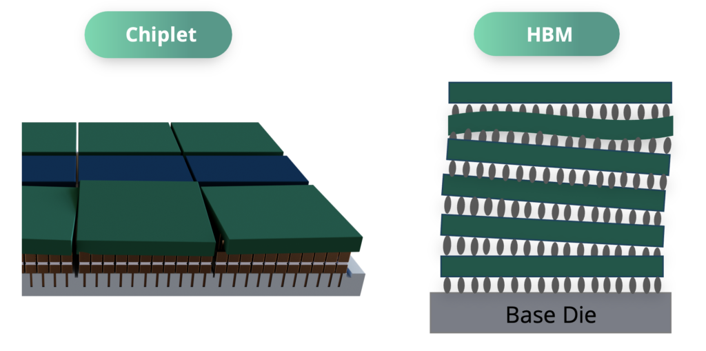
The Shift to Chiplets and HBM
AI accelerators rely on Si interposer and chiplet architectures, where multiple smaller dies are interconnected instead of using a single large processor. This approach enhances scalability, increases yield, and improves energy efficiency. HBM technology, integrated via silicon interposers or embedded bridges, enables faster data transfer and reduces latency—key factors in AI performance.
The Role of Inspection and Metrology
To ensure reliability, every step of advanced packaging involves meticulous inspection and metrology. Key areas include:
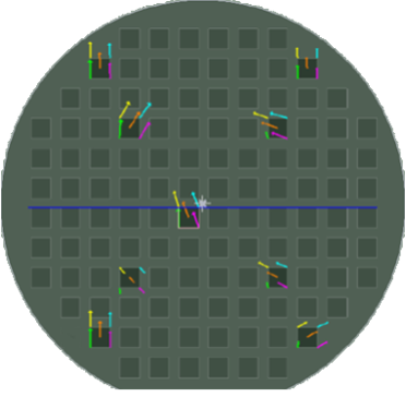
- Bump Height Metrology – Precise measurements of hundreds of millions of chip interconnects ensure reliable electrical contact.

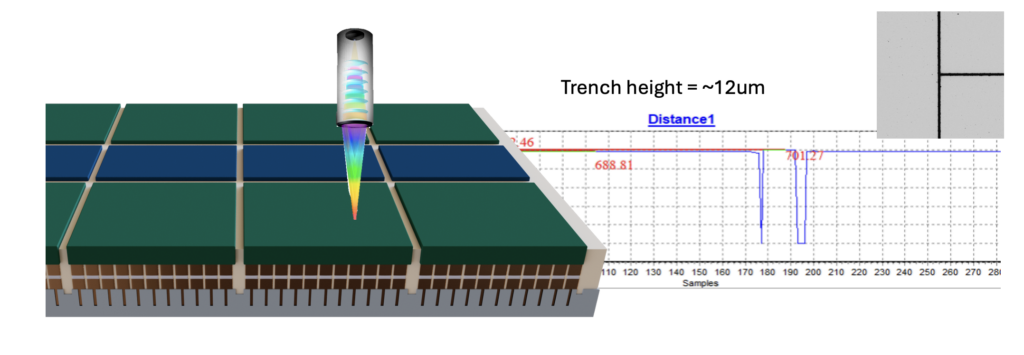
Figure 1: Application results of interconnect (bump) field measured with Camtek’s Triangulation Sensor. - Warp and Tilt Inspection – Detecting die warp and misalignment during stacking prevents failures in multi-layer HBM structures.

- Underfill Defect Detection – Excess epoxy can damage mold coatings and impact overall chip integrity.
The Future: Hybrid Bonding and Miniaturization
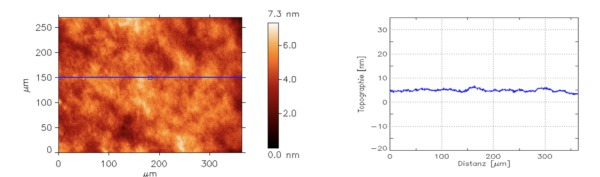
As interconnect densities increase, traditional solder bumps are being replaced by hybrid bonding techniques, which enable direct oxide-to-oxide connections. This shift significantly enhances memory capacity and processing speed but introduces new metrology challenges, such as detecting microscopic defects and ensuring ultra-flat surfaces.
This technology shift requires new inspection and metrology capabilities:

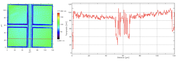
- Surface Roughness Metrology – Hybrid bonding requires ultra-smooth oxide surfaces, down to nanometer level, for successful interconnection.
- Overlay Metrology – Achieving sub-micron precision in die-to-wafer or wafer to wafer bonding is crucial for next-generation packaging.
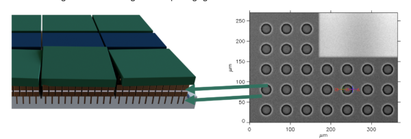
- Cu Pad Dishing Metrology – Measurement of sub-nano dishing is important for validation of interconnect reliability at HVM and quality control feedback for CMP process.
Camtek’s additional capabilities for chiplets and hybrid bonding cutting-edge heterogenous integration processes:
- High AR TSV depth metrology
- Edge and bevel inspection and metrology
- 150nm defect detection
- Die stack thickness metrology
- Thin layer thickness metrology
Camtek is at the forefront of these advancements, developing high-precision inspection and metrology solutions to meet the demands of next-generation semiconductor manufacturing. With technologies like white light interferometry (WLI) for nano-topography analysis, infrared-based overlay metrology and thin film reflectometry for the determination of transparent thin layers and layer stacks the company is helping drive the AI revolution forward.
As AI continues to evolve, so will the need for precision in semiconductor manufacturing—ensuring that every chiplet and memory module meets the highest standards of performance and reliability.


