


The semiconductor industry is rapidly advancing, with an increasing emphasis on cutting-edge packaging techniques such as heterogeneous integration (HI), 3D heterogeneous integration (3DHI), and chiplets. These innovations necessitate efficient, cost-effective, and damage-free debonding processes to ensure high-yield manufacturing. Conventional mechanical and laser-based debonding methods often introduce challenges such as thermal stress, contamination, and high operational costs. In contrast, photonic debonding, which utilizes high-intensity broadband light pulses in conjunction with an inorganic light-absorbing layer (LAL), has emerged as a transformative technology, delivering numerous advantages across semiconductor manufacturing.
What is Photonic Debonding?
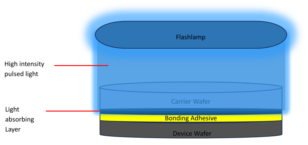
Photonic debonding (Fig. 1) employs intense, short-duration (µs) pulses of broadband light to induce vaporization at the adhesive-LAL carrier wafer interface, creating an air gap that facilitates stress-free separation. Unlike laser debonding, which can induce localized heating and thermal stress, photonic debonding ensures uniform energy distribution across the substrate and the inorganic LAL, eliminating light-induced wafer damage. This approach is particularly valuable in handling ultra-thin wafers in advanced semiconductor manufacturing, neuroelectronics and solar cells, and energy applications.
Key Benefits of Photonic Debonding
Lowest Cost per Wafer
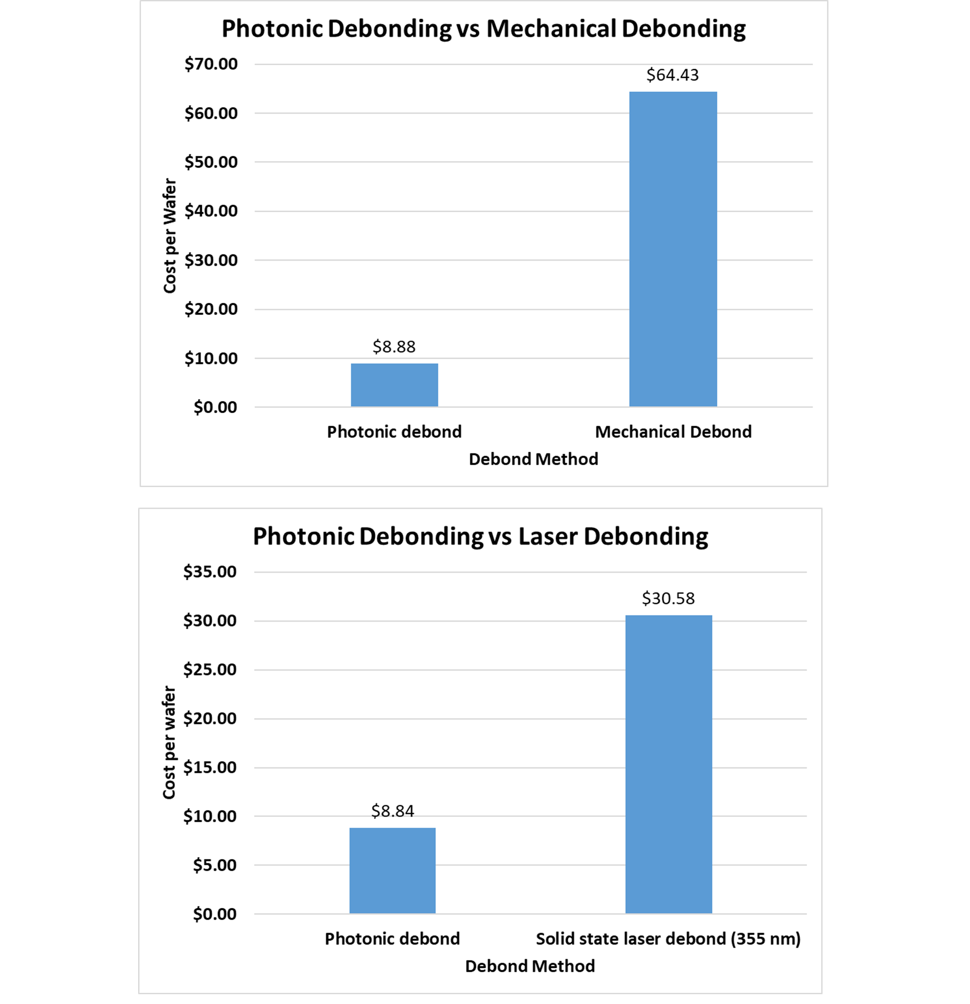
Photonic debonding offers the industry’s lowest processing cost per wafer with improved yield. It reduces processing costs by eliminating the need for single-use carriers and sacrificial polymer layers. Traditional debonding techniques often require extensive post-processing and disposable materials, increasing processing costs. With its high throughput and minimal consumable usage, photonic debonding further enhances cost efficiency. Compared to conventional laser and mechanical debonding, it reduces the cost per wafer by over 80%, with $5M+ savings for every 100k wafers processed (300 mm) in high-volume manufacturers (Fig. 2).
Facilitating Ultra-Thin Wafer Processing
Modern semiconductor applications demand ultra-thin wafers, particularly for 3D wafer stacking and heterogeneous integration. Conventional mechanical debonding methods can introduce stress-related warping and cracking, rendering them unsuitable for delicate wafers, especially when they are thinned below 30 µm. Photonic debonding with its low-stress carrier separation and low thermal impact to the thin wafers has successfully demonstrated debonding <20 µm repeatedly over several lots of wafers, improving yield and reliability.
Improved Yield and Process Reliability
Ensuring high-yield manufacturing is a major challenge when working with delicate substrates. Photonic debonding’s non-contact, stress-free mechanism minimizes defects and enhances overall process reliability. Unlike mechanical methods that rely on force or thermal cycling, photonic debonding prevents microcracks, contamination, and yield losses associated with excessive handling. PulseForge in collaboration with Applied Novel Devices demonstrated 100% yield of Silicon Power MOSFETs undergoing back-grinding and back-side metallization and they debonded using photonic debond. [1]
Seamless Compatibility with Hybrid Bonding
Hybrid bonding, which integrates dielectric and metal bonding, is crucial for next-generation semiconductor devices. Photonic debonding offers a cleaner debonding process, reducing polymer residues and contaminants that could compromise hybrid bonding integrity. Adeia Inc., presented a paper on employing photonic debonding with efficient polymer cleaning on the device wafer to improve yield in hybrid bonding enhancing bonding reliability and electrical performance. [2]
Higher Throughput and Faster Processing Time
Time efficiency is critical in high-volume semiconductor manufacturing. Mechanical and thermal debonding processes often require lengthy heating and cooling cycles. In contrast, photonic debonding pulses light in durations of microseconds. Its large-area illumination capability surpasses that of laser debonding, enabling high-throughput processing of wafers or panels. Throughput improvements of more than 5X compared to traditional methods have been demonstrated by the fully automated tools.
Scalability for High-Volume Manufacturing
As semiconductor packaging moves towards high-density integration, scalable debonding solutions are essential. Photonic debonding seamlessly scales to high-volume production environments, accommodating large wafer sizes and diverse substrate materials. Its ability to process over 70 wafers per hour enhances manufacturing efficiency, making it an attractive choice for semiconductor foundries, integrated device manufacturers and outsourced semiconductor assembly and test (OSAT) facilities.
Minimal Thermal Stress and Warpage Prevention
Temperature-sensitive devices, including compound semiconductors and delicate MEMS wafers, require low-thermal-impact processing. Laser-based debonding methods can introduce localized heating, leading to thermal stress and warpage. Photonic debonding minimizes thermal exposure by delivering ultra-fast energy pulses that selectively interact with the light-absorbing layer, ensuring uniform, low-stress debonding.
Sustainability and Eco-Friendliness
The semiconductor industry is increasingly adopting sustainable manufacturing practices. Traditional debonding methods often involve hazardous chemicals, high energy consumption, and disposable materials. Photonic debonding significantly reduces the need for solvents, reduces waste from single-use carriers, and operates with energy-efficient pulsed light technology. It contributes to green manufacturing initiatives by reducing chemical waste by at least 50% and energy consumption by over 90 %.
Enabling Advanced Applications: MicroLED, Battery Technologies and 2D Materials
Beyond semiconductor packaging, photonic debonding is gaining traction in emerging applications such as MicroLED mass transfer, battery technology and 2D materials. MicroLED displays require precise and damage-free release processes to achieve high pixel density and defect-free integration. Similarly, photonic debonding enables the residue-free release of thin film layers without mechanical stress. PulseForge and imec collaborated to demonstrate defect-free transfer of 2D materials using photonic debonding and demonstrated yield improvements of >99.5% further underscoring its benefits.

Key Applications of Photonic Debonding
Semiconductor Packaging
- Wafer-Level Packaging (WLP): Supports thin wafer handling for Through-Silicon Via (TSV) creation, silicon interposer manufacturing, and fan-out WLP.
- 5D & 3D Heterogeneous Integration: Enables stacking of multiple dies for high-performance computing and AI applications, including CoWoS, Foveros, and interposer technologies.
- High-Bandwidth Memory (HBM): Facilitates DRAM die thinning, essential for next-generation memory architectures.
- Hybrid Bonding: Enhances wafer-to-wafer and die-to-wafer alignment while ensuring clean separation of temporary carriers.
Compound Semiconductors & Power Devices
- GaN, GaAs, and SiC Power Devices: Supports thin wafer processing, back grinding, and back-side metallization for high-power applications.
Photonics & Optoelectronics
- Silicon Photonics: Enables thin-film handling for optical waveguides and laser integration.
- Image Sensor Manufacturing: Enhances CMOS image sensor fabrication by enabling wafer thinning and filter array transfer.
MEMS & Neuroelectronics
- MEMS Devices: Facilitates fabrication of accelerometers, gyroscopes, and pressure sensors.
- Brain-Computer Interfaces (BCIs): Enables clean separation of flexible implants from temporary carriers.
Advanced Materials & Energy Applications
- Graphene & 2D Material Transfer: Achieves clean transfer with over 99.5% yield.
- Solid-State Batteries: Enables residue-free release of thin film layers.
- Thin Solar Cells: Supports thinning and separation using temporary carriers for high yield without degradation.
Conclusion
Photonic debonding represents a paradigm shift in semiconductor manufacturing by addressing key challenges associated with cost, yield, and scalability. By delivering a stress-free, rapid, and contamination-free debonding process, photonic debonding enhances process reliability and enables advanced packaging applications such as 3DHI, hybrid bonding, and ultra-thin wafer handling. As semiconductor manufacturing continues to evolve, photonic debonding will play an increasingly vital role in enabling next-generation technologies, reinforcing its position as an indispensable tool in the semiconductor industry.
References
[2]. https://virtual.oxfordabstracts.com/event/73607/submission/130 (Presented at IMAPS DPC 2025)


