


3D integration is becoming a valuable alternative to the ongoing, yet challenging, transistor scaling known as Moore’s Law. This is especially true for semiconductor products that are becoming limited by single die designs (e.g., in terms of form factor, size, and technology node).
Homogenous 2.5D-IC approaches help bring about the era of chiplets—with its great emphasis on IP reuse. Additionally, heterogenous integration allows different process nodes to be mixed in the same semiconductor product. In terms of 3D-IC design enablement, reliability analysis is becoming of great importance.
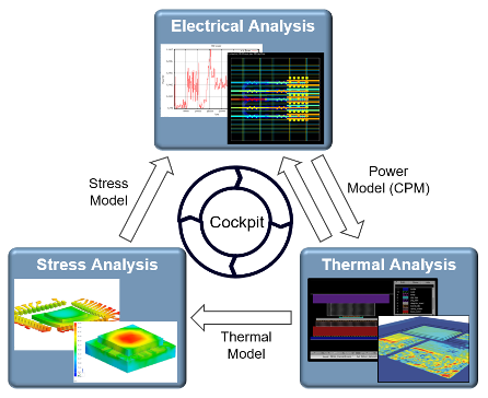
When it comes to 3D-IC reliability, electrical analysis, thermal analysis and stress analysis can’t be treated as independent variables anymore. That is, thermal issues affect stress behavior since the difference in thermal expansion coefficients (CTEs) between substrates results into warpage. Stress issues affect electrical behavior since electrical devices behave differently under different stress conditions. Finally, thermal issues affect electrical behavior since the heating of interconnects affects wires resistivity. As can be seen, electrical, thermal and stress analysis are now highly correlated which results into a “multi-physics” challenge that needs to be addressed by EDA.
Since 3D-IC system level designers are not expected to be domain experts in electrical analysis, thermal analysis and stress analysis, a system level EDA cockpit is needed. At IMAPS DPC, Siemens presented on a system level cockpit that the designer (typically with an electrical engineering background) can use to create the 3D-IC system level model and automate the required setup for each domain analysis (physical verification, electrical power analysis and thermal analysis). This enables the designers to run “what if” analyses iterations and make design related decisions early enough where system design changes are feasible and not costly.
The importance of multi physics analysis for STCO
SoC (homogenous) design is a well-established process in which there is minimum interaction between die design flow and package design flow.
Heterogeneous integration is a very different problem in which the designer needs to worry about the system level interactions between the different components of a 3D-IC design. The traditional term for this used to be “die/package co design”. Currently, a more comprehensive wording is “system technology co optimization” (STCO).
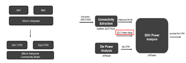
A chiplet is a die that is designed/optimized to be integrated with other die(s) in an advanced package/3D-IC. For every chiplet, the designer still needs to do the traditional die design and sign off so the chiplet is fit for purpose and manufacturable. Then, the designer needs to look at the substrate design and signoff. The substrate is basically the “interconnect” that connects the different chiplets together. It can be an interposer (silicon or organic). Once this is done, the designer needs to take care of the system-level planning and sign off that usually happens across multiple design domains/teams. Finally, we have the system-level “multiphysics” analysis the needs to account for die, package and in-system interactions.

Multi physics is defined as the simultaneous simulation of different aspects of a physical system (or systems) and the interactions among them. In simple words, multi physics means that thermal, electrical and stress behaviors of an advanced package/3D-IC are not independent variables anymore. The thermal behavior affects the stress behavior due to the different thermal expansion coefficients between the different material (for ex: die (silicon) on an organic interposer) which results into potential warpage.
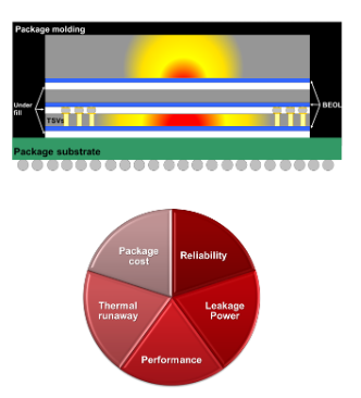
The stress behavior affects the electrical behavior since the transistors behave differently under applied stress. Also, the thermal behavior affects the electrical behavior because when the wires heat up, their resistivity change. As can be seen above, we start to see this circular behavior between the different types of analysis. The user needs a software platform that can act as the “cockpit” the manages these different types of simulations.
Then, we have the 3D-IC system level designer in the middle of these different type of analysis. this is someone who often has an EE or ME background (not both!). Although it is not practical to assume that he/she is an expert in every verification/analysis flow, he/she still needs to take “system level” decisions. For example, the 3D-IC technology vendor, the substrate type (silicon interposer, organic interposer, etc. …), the Die(s) floor planning decisions, etc. … He/she also needs to take these decisions as early as possible before the cost of change is too high.
The challenge of multi physics analysis for 3D-ICs requires a cockpit software platform that can manage the different types of the analysis. The cockpit should have a full understanding of the system so that it can partition any part of it and export the needed data for every domain specific analysis. Siemens offers Innovator3D IC platform that enables an automated setup generation for every respective tool/analysis.


