


Is TSMC Acquiring 20% of Intel fabs?
Reports are that Intel and TSMC have reached a preliminary agreement to form a joint venture that will operate Intel’s manufacturing facilities. TSMC will hold a 20% stake in the new company.
The news comes from Reuters, which cites a report from “The Information” based on “…two sources familiar with the matter”. Intel has not yet commented on the matter. TSMC declined to comment.
At present it is unknown which companies will own the remaining 80% of the venture. Earlier this year TSMC reportedly approached multiple fabs including AMD, Broadcom, Nvidia, and Qualcomm about investing in such a venture.
The current US administration reportedly initiated the talks between the two semiconductor giants in an effort to prop up Intel, which has had significant manufacturing issues in recent years. Reports speculate that TSMC pitched the idea of a joint venture to Nvidia, AMD, and Broadcom, following a request from the U.S. administration to assist in Intel’s revival.
Questions remain about how the two companies would integrate their operations, given that they use different production equipment models and materials. Many of Intel’s fabs can only be used to make processors for Intel (including fabs capable of producing on Intel 3 and Intel 4 process technologies) and only one or two of which can make processors on Intel’s 18A fabrication technology.
It is also being reported that instead of funding its stake with capital, TSMC will share some of its chipmaking practices with Intel employees and train them.
Is Panel-level packaging (PLP) finally emerging?
Gabriela Pereira of Yole Group recently put out a white paper highlighting their 2025 report “Panel level Processing 2025” dealing with the emergence of panel level processing. Let’s take a closer look.
Despite its significant advantages, there have been widespread challenges to the widespread adoption of PLP. Its main driver is reported to be cost reduction. The large area of PLP enables higher manufacturing throughput, theoretically making it a better solution for high-volume production. Additionally, the rectangular shape of panels offers improved manufacturing efficiency, particularly for larger package sizes as shown in Figure 1.
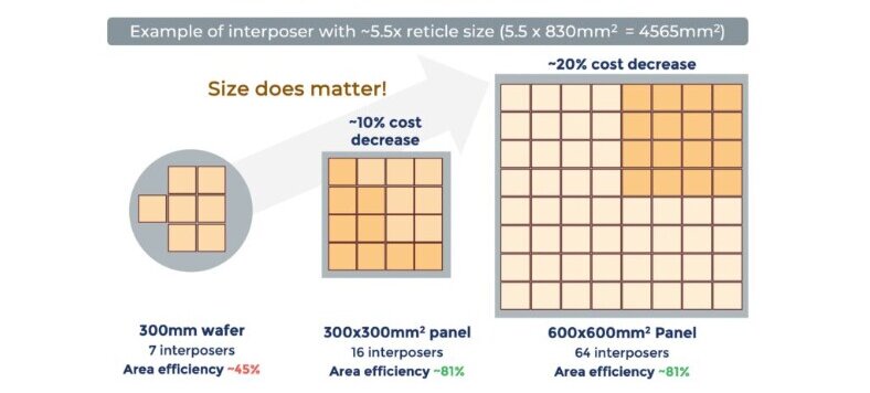
In terms of advanced packaging technology, silicon interposer technology has reached its reticle size limit, prompting an intense look at organic interposer options for larger package sizes.
PLP issues come from both economic and technical perspectives. Large investments are needed to develop panel lines, and that investment is justified only for high-volume applications. Yole concludes that “For small-package, low-volume applications, WLP can remain the most practical solution, limiting PLP potential.”

In addition, current PLP processing still struggles to achieve the same level of resolution as WLP. While advanced lithography equipment reportedly can achieve 2/2µm line and space resolutions in panels, replicability at high volumes with acceptable yields remains a challenge. Other technical challenges include panel warpage, die placement accuracy, and overall yields. Without sufficient yields, overall panel cost savings cannot be realized.
Market Status
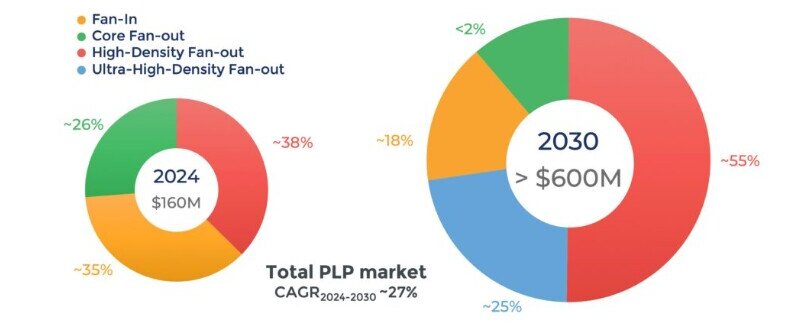
Yole analysts estimate that in 2024, the total PLP market achieved about $160 million of revenue and a global production of almost 80 thousand panels (~330 thousand equivalent 300mm wafers). And by 2030, this market could reach more than $650 million and a volume of approximately 220 thousand panels.
Companies like Samsung, PTI, Nepes, ASE (with Deca as the technology licenser), SiPLP and STMicroelectronics (with PEP as a technology licenser) have reportedly been manufacturing PLP in recent years.
While Samsung has been using PLP for mobile and wearables application processors, the others have been focusing on small package applications like PMIC and other power ICs, RF, and MCU devices, mainly for the mobile and consumer space.
Established PLP players like PTI, Samsung, and ASE, along with newcomers like Amkor, Innolux, ECHINT, Rapidus, Silicon Box, and even TSMC, have been closely following this trend and have started developing PLP technology for large, high-end fan-out packaging. TSMC’s public announcement of its development of PLP has been drawing significant industry attention. Yole anticipates that TSMC’s technology may be developed within the next three years although did note share what led to this conclusion.
For all the latest in advanced packaging stay linked to IFTLE…………………………


