


In today’s digital world, the demand for more powerful, efficient, and compact electronics is surging. With every leap in performance and shrinking chip size, the pressure is on for manufacturers to adopt cutting-edge metrology solutions that can keep pace and ensure flawless quality even as production volumes soar.
Here, Ben Peecock, Director of Business Development, X-Ray & Test at Nordson Test & Inspecton, explores how automated x-ray metrology is providing game-changing quality and efficiency in wafer and panel level applications, and delves into some of the trends shaping the industry.
X-ray insight: the crucial role of metrology in the innovation race
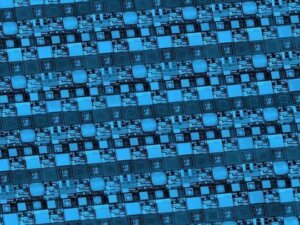
Behind the devices we use every day is a world of advanced manufacturing to develop the electronic components – right down to the intricate production of the semiconductor chips and their constituent parts. The importance of inspection and metrology within this production process has long been recognized; these systems are the backbone of quality control, ensuring that devices meet exacting tolerances and catch defects early to optimize yields and reduce waste.
Today’s hyper-competitive market and pace of innovation brings new challenges, including tighter margins and pressures for manufacturers to improve their products while pushing the boundaries of miniaturization and power. As chips become smaller and mightier, manufacturers have been forced to adapt and embrace new, cutting-edge inspection technologies. With smart technologies increasingly utilized in the most high-stakes of applications from automotive to aeronautics, the demands on modern electronics – and therefore on quality control within electrical component manufacture – have never been greater.
X-ray metrology is increasingly being implemented to ensure precise measurements, early defect detection, and process optimization. This technology has become particularly important in wafer and panel level applications, where traditional methods can struggle to keep up with the complexity and miniaturization of modern chips. While other inspection methods can provide information on external properties or detect simple internal voids, x-ray metrology delivers a highly detailed 3D image of the internal structure, enabling the identification of numerous issues from air gaps and wafer fractures to solder bump defects or thickness variations. By unlocking this level of detail, manufacturers can drastically improve yields, reduce false call rates and minimize the time and resources wasted in processing defective chips, all while keeping pace with the acceleration towards advanced chip packaging.
The advantage of automated x-ray metrology inspection
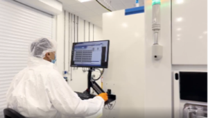
Although x-ray metrology unlocks some of the primary challenges facing semiconductor manufacturers, the true potential of this technology is realized when we embrace automation. By automating the x-ray inspection process, manufacturers enjoy enhanced throughput, allowing for inspection of a far greater volume of wafers and panels in less time. This acceleration streamlines production and reduces the chances of human error, ensuring measurements are consistent and reliable. Furthermore, automated systems provide real-time data analysis, permitting manufacturers to instantly detect defects and immediately adjust production. This approach both further improves yield and minimizes waste, contributing to a more efficient and cost-effective operation.
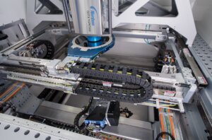
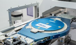
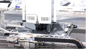
Solutions like our XM8000 platform have successfully integrated leading x-ray technology with high-level automation to provide a high-throughput operator-free system for TSV metrology, wafer-level packaging analysis and defect review. By combining these capabilities with the advanced science, in-house manufactured parts and our own sophisticated software, we are pioneering not just enhanced workflows but enhanced processes and end results. In a landscape where precision and speed are paramount, this technology becomes a core, irreplaceable pillar of the production floor, enabling manufacturers to unlock a new level of excellence in quality assurance and ultimately help drive the industry forward.

Scanning the horizon: The future of semiconductor inspection
With the continued evolution of semiconductor manufacturing and inspection, there are a several emerging trends and developments set to drive industry transformation. One of the most intriguing advancements is the exploration of glass as an alternative to silicon in wafer production. Unlike silicon, which naturally forms in a circular shape, glass can be manufactured in squares, maximizing surface area and allowing more chips per wafer. This shift could dramatically boost chip yield, resulting in more powerful and cost-effective products.
Equally transformative is the growing integration of AI and machine learning into inspection systems. As these technologies become more deeply embedded in manufacturing, we are naturally tapping into vast amounts of data that can be leveraged in the systems’ evolution, driving continuous improvement.
With AI learning at an exponential rate, fully automated production and quality control processes are almost within reach – with systems that adapt, refine, and optimize themselves without human intervention. There’s no doubt that rapid growth of AI and machine learning is geared to redefine production across the board and semiconductors are no exception.
Finally, as devices become increasingly powerful and demand for higher performance rises, the shift from traditional single-layer wafers to multilayer panels is gaining momentum. These advanced architectures support the growing complexity of chip design, offering more processing power in smaller footprints.
Looking ahead, the role of automated x-ray metrology in ensuring product quality and reliability cannot be overstated. The technology is key in building a future where semiconductor manufacturing is not only faster and more efficient, but also capable of meeting the demands of next-generation products with remarkable precision and agility. From detecting subtle defects to providing detailed imaging of complex structures, x-ray metrology is essential for maintaining the high standards required in wafer and panel level applications. As we continue to see significant bounds in technological advancement, our ongoing work to continue advancing our systems and delivering better image quality, superior post-processing capabilities and higher failure detection rates will only become more critical in helping manufacturers meet the challenges of tomorrow.


