


By Tony Mastroianni and Todd Burkholder, Siemens DIS
Over the last several years, chiplet-based heterogeneous package integration has emerged as a promising alternative to traditional monolithic package solutions; the so-called homogenous SoC design. 3D IC heterogeneous integration is a system approach, wherein what typically would be implemented as an SoC is disaggregated into solid, fabricated IP blocks; i.e., chiplets.
These chiplets typically provide a specific function implemented in an optimal chip process node. Several chiplets and an optional, custom SoC device can be mounted and interconnected in a single package using high-speed/bandwidth chiplet-to-chiplet interfaces. The resulting 3D IC heterogeneously integrated packages deliver greater performance at a reduced cost, higher yield, and have only a slightly larger area than a traditional monolithic SoC package.
This system-oriented approach, known as system technology co-optimization (STCO), differs from traditional IC design. STCO spans five significant activities that are both complex and sophisticated: architectural planning and analysis, functional design and test, physical design planning and verification, and electrical and reliability analysis.

With this new approach come many advantages, opening new possibilities in electronic system design; however, the question facing us is how to facilitate the adoption of this exciting yet esoteric 3D IC methodology, one requiring a high degree of expertise and effort.
With that quest in mind, in 2021, the Chiplet Design Exchange (CDX) was established within the Open Compute Project (OCP) to promote and support this technology and eventually deliver it to the mainstream. The CDX group comprises EDA vendors, FABs, OSATs, and substrate material providers. The charter of the CDX group is to promote a chiplet ecosystem by defining models that are necessary to support the 3D IC design process, as well as the different types of design kits that this requires. Therefore, we set out to establish an ecosystem of design kits to enable 3D IC design throughout the semiconductor industry and address the fact that the packaging community has lacked the well-structured design kits and PDKs available for traditional ASIC technologies.
The idea was that we could eventually have reusable chiplets out in the marketplace, and that’s what we’re promoting in the CDX group. Therefore, it was critical to develop and leverage existing standards for the various 3D IC design kit formats (which we call 3DKs), and we wanted the 3DKs to be in machine-readable formats that can be consumed by the tools and the workflows. In turn, we needed to have the EDA companies support these workflows and the different formats. Finally, to make the critical link to manufacturing, the OSATs —the foundries that generate the data for these different design kits—also had to be part of this ecosystem.
The 3DKs: 3D IC Design Enablement
As mentioned, the IC design process has a very structured, well-defined design enablement infrastructure. It includes IP: the reusable building blocks of SoC designs. There are process design kits, which include the technology rules for creating extraction decks, place and route decks, et cetera. There are also macros for memory and analog signal-type designs. We’re trying to extend that concept for many things in the packaging world, but a different set of design kits is required. So, 3D IC design requires a comprehensive set of new design enablement kits to support the design, verification, and handoff to manufacturing.
These design enablement kits fall into five key areas, as reflected above. These are physical design, electrical analysis, reliability analysis, and test that start up front during planning. Also, as parts are delivered for manufacturing, test factors both for the individual chiplets as well as the complete system-in-package (SiP) must be generated.
To support the needs in all these key areas, we are developing four 3DKs to provide a comprehensive set of design enablement kits that support the design, verification, analysis and testing of 3D IC designs.
- Chiplet Design Kits (CDK): Recommended chiplet models to support the integration into a 3D IC design
- Package Assembly Design Kits (PADK): Chiplet IO/TSV pitch spacing rules, substate/interposer width/spacing, routing rules, and general-purpose package component placement rules
- Material Design Kits (MDK): Composite material properties for package components to support electrical and reliability analysis
- Package Test Design Kits (PTDK): Defines test IO pins, dimensions, and function to support ATE test hardware and testing
Chiplet Design Kits
CDK models are created or reused for early architectural, test, and physical design planning. These are the models that are required to design a chiplet. So, the first thing the CDX group did was determine the design models required to integrate a chiplet into a package. Our first effort involved working with the JEDEC group.
The JEP30 Part Model was designed to describe electronic components used in a PCB design. As we were trying to do a similar thing for 3D ICs, we asked them to help us extend that part model to support chiplets. Together we came up with a list of chiplet design models that we recommend be included with a chiplet. The idea is that we could eventually have reusable chiplets out in the marketplace. And we drove that extension to the JEP30, the Part Model, back in January of 2023. That is now a JEDEC standard.
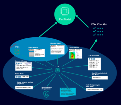
We next developed checklists for other formats and recommended the models required to support design analysis. At a minimum, we have a checklist to know what models are available. A chiplet designer or chiplet provider can define which models are available. There are also provisions where we can include the models, and that’s really up to the chiplet provider if they want to include that in the part model.
Package Assembly Design Kits
Today we are actively working on the package assembly design kits. These include the rules for defining pitch, spacing, and the type of connectivity components used to connect the chiplets to the interposers and substrate.

In keeping with our guidelines, they are in a machine-readable format, and they are EDA-neutral. Thus, each of the EDA vendors, assuming they’re supporting these formats, would be able to take those rules from a single source. This results in much cleaner access for the FABs and the OSATs during manufacturing, because they can provide these rules in one format that all the EDA tool vendors can use. With access to this information and these machine models, the PADKs can be used for scripting directly in some of the EDA tools.
Material Design Kits
Another area we are working on is material design kits. These are a truly novel idea. When engineers are doing analysis—whether it be thermal, stress, signal integrity, or power integrity — the MDKs can define the material properties that are in the package components inside the package. Again, the idea is to put these in a machine-readable format, rather than having that information derived ad-hoc from the vendors and material providers and manually input into the tools. Then the tools would use the MDKs to use that material information directly for analysis.
Package Test Design Kits
As the name implies, package test design kits are for test. The chiplet model contains a lot of information in terms of the physical dimensions of the device, also the pins, and the functional mode. But when you’re testing these devices, typically there is a different set of pins that are used to test for wafer sort when you’re testing the wafers. The PTDKs define the location of those pins, the modes, the physical location, the shapes, and all the geometries.
Workflows to Support 3D IC
Another benefit of a Part Model, and one of its targeted purposes, is to enable a chiplet market ecosystem. Chiplet suppliers can design a chiplet, and if they want to offer that to the market, they can describe all the required information and make it available.
This gives chiplet suppliers the ability to define essentially the information about their products in an electronic catalog, in which designers can see the different available parts and choose the ones best suited for their particular design.
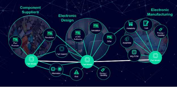
Thus, chiplet providers can empower prospective customers to search for their chiplet IP and assess functionality, detailed electrical/physical attributes, and available design models. System designers and chiplet consumers can then look through that catalog and also do business transactions. Finally, the 3DK models can be used for the design and verification process, and eventually handed off to manufacturing.
Lastly, we are advancing the development of the authoring tools required to create these models. The 3DK models are in CDX format, and this is not a friendly format for someone to type, so there is a need for an open-source EDA-neutral authoring tool. The goal is to have a single tool that will create each of these 3DK models, and the specific EDA vendors, manufacturers, and assemblers would then use the EDA-specific implementations to create the decks, etc. Toward that end, Siemens EDA introduced Innovator3D IC. Innovator3D IC offers a comprehensive multi-physics cockpit for 3D IC design, verification, and manufacturing to deliver a fast, predictable path for the planning and heterogeneous integration of ASICs and chiplets.

As this article has attempted to show, the CDX working group has been hard at work to provide the open source, EDA neutral, machine-readable 3DKs and chiplet authoring tools that will propel 3D IC heterogeneous integration into the mainstream of electronic systems design. And we’ll be coming to your town very soon.
Tony Mastroianni, co-author of Taking 3D IC Heterogeneous Integration Mainstream, is the Advanced Packaging Solutions Director at Siemens Digital Industries Software. He has more than 30 years’ experience as an engineer and engineering manager in the global semiconductor industry and currently leads development of advanced packaging solutions for Siemens EDA. Prior to joining Siemens, he served in engineering leadership positions at Inphi and eSilicon. Tony earned a B.S.E.E from Lehigh University and a M.E.E at Rutgers University.
Todd Burkholder, co-author of Taking 3D IC Heterogeneous Integration Mainstream, is Senior Writer and Editor at Siemens DISW, working with SMEs and customers to create content for the majority of EDA technology divisions at Mentor Graphics and Siemens from 1997 on. He began his career in high-technology marketing in 1992 after earning a Bachelor of Science at Portland State University and a Master of Arts degree from the University of Arizona.
Editor’s Note: This article first appeared in the 2025 3D InCites Yearbook. Read the issue here.


