


Artificial intelligence (AI) is driving the need for faster processing speeds to keep up with the large language models. As a result, we see multi-reticle packages using 2 x 800 mm2 chips in production in a single package. These larger chip sizes and the need for better yields and higher capacity drive the move from wafers to larger rectangular substrates for the packaging process. The move to fan out panel-level packaging (FOPLP) is partly driven by the industry’s move to packaging chips on a substrate to reduce the limitations and constraints of the wafer-level packaging process. The rapid adoption of multiple-reticle chiplets has created packaging shortages as the FOWLP packaging process is capacity-constrained due to the large size of these packages.
To improve the capacity situation, packaging companies are working to develop panel-level packaging (PLP). Instead of using a round wafer in the packaging process, a square substrate will be used for PLP. AMC Research (AMCR) has a long history of success with wafer-level packaging (WLP), and it is supporting the transition to PLP with new approaches for cleaning and deposition technologies. Before we move into some details of PLP, however, let’s discuss why we need to move to larger substrates in the first place.
Large-package Design Challenges
Building packages that are larger than 2 x 800 mm2 has multiple challenges. One of the biggest issues is how many 800 mm2 chips can be placed on a 300 mm wafer or packaging substrate. With a chip size of ~800 mm2, about 64 chips can fit on a round 300-mm wafer. However, this does not consider yield. The chip is square and the wafer is round, so a significant amount of substrate goes to waste in the chip’s processing. This is because a considerable amount of area at the edge is lost due to the mismatch in shape.
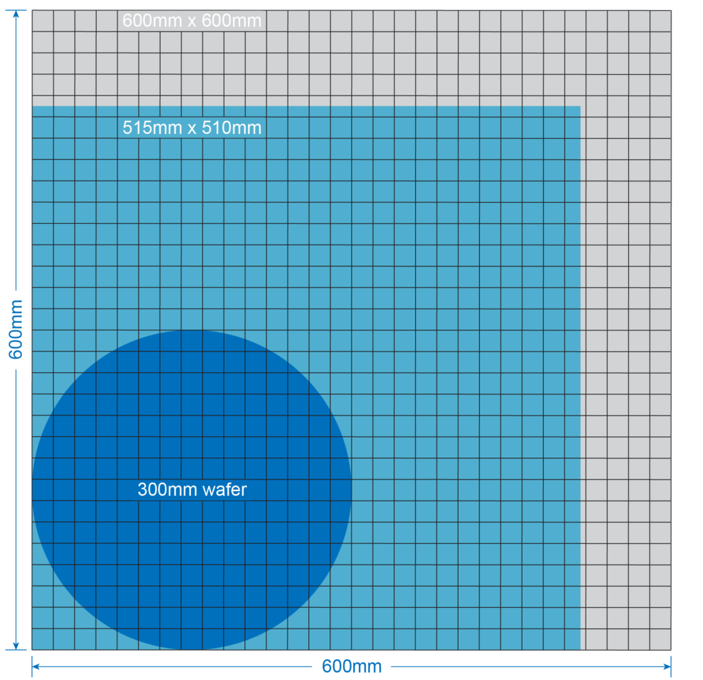
To help resolve packaging supply chain constraints, the packaging industry is moving from round substrates to square panels. Both wafer manufacturers and outsourced assembly and test (OSAT) packaging suppliers have proposed using square glass panels as the substrate for packaging the large-area chiplets. This will significantly increase the number of chips that can be processed on a single panel and should ease current supply constraints. The industry for now has settled on panel sizes of 515 mm x 510 mm, which has 3x the area of a 300 mm silicon wafer; and 600 mm x 600 mm, which has 5x the area of a 300 mm wafer (Figure 1).
Advantages of Panel-level Packaging
Transitioning to PLP has some advantages over WLP. For example, PLP enables the industry to significantly increase the substrate area for building chiplets, improving yield and lowering packaging costs. The larger area allows more chips to be assembled simultaneously, increasing capacity and thus reducing the current supply constraints. FOPLP will allow for the integration of various die technologies (e.g., logic, memory, and RF) more easily in a single package, which supports more complex system designs. By utilizing fan-out techniques, designs can be made thinner and smaller, which is essential for modern consumer electronics. PLP integration can improve chiplet performance for the massive amounts of data being processed by AI, as well as in other compute-heavy applications. PLP also assists with the implementation of high-bandwidth memory (HBM) to help reduce compute times and power usage. Implementing PLP will also allow for more efficient package device design, as opposed to the more typical board-level packaging approach, which is the direction the industry is heading.
Enabling the Transition

New process equipment and panel handling is needed to make the transition to PLP. For example:
- Electroless and electrolytic plating will be critical in building up the redistribution (RDL), pillar, and bumping layers to create the interconnects needed.
- Panel bevel etching and cleaning in copper-related processes for both the front and back of the panel will help improve yield and remove metal contamination and residues that could cause electrical shorts.
- A panel cleaning tool is needed that can remove flux and contamination from the center of the panel to eliminate void formation and prevent shorts.
- And finally, a flexible panel handling system is required that can manage thin wafers and panels.
ACM Research has developed process tools and substrate-handling systems to address these critical PLP process components to drive the future of packaging forward.
Summary
The transition from WLP to FOPLP reflects the industry’s need for cost-effective, high-performance solutions that can meet the demands of modern electronics. As technologies evolve and the demand for smaller, more powerful devices increases, ACMR has been working with the industry to develop technology that will help FOPLP play a significant role in the future of semiconductor packaging.
This article first appeared in the 2025 3D InCites Yearbook. Read the full issue here.


