


An Intel engineer holds a test glass core substrate panel at Intel’s Assembly and Test Technology Development factories in Chandler, Arizona, in July 2023. Intel’s advanced packaging technologies come to life at the company’s Assembly and Test Technology Development factories. (Credit: Intel Corporation)
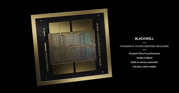
TSMC has announced a roadmap to 9 reticle packages to meet the demand for large scale systems in a package. (A multi-reticle package has more than 800mm2 area of chips in the package.) Nvidia’s Blackwell currently has two chips slightly larger than 800mm2 in the package with eight stacks of HBM, giving each package 193 GB of memory.
This year (2025), TSMC is expected to introduce a 6X reticle-size super carrier interposer to improve the manufacturing process and yield of the multi-reticle packaging process. TSMC reports that the interposer size could reach 5148 mm2. Last month, we reported that 9X reticle packages are slated for 2027.
The COWoS-L process still uses conventional packaging technology, which means round substrates are used to prepare the chips for packaging onto the interposer. Using a round packaging substrate means you can fit roughly 64 dice onto the substrate. A round substrate limits throughput and can introduce yield challenges. The industry has recognized the substrate limitations and has been working towards square substrates that can increase the throughput and potentially increase yield, as more square dice can be placed onto a square substrate than a round substrate. Fraunhofer IZM has been working on square substrates or panel level processing (PLP) since 2016 with 17 international partners. The work on large substrates has grown with TSMC, Intel, and others developing processes and technology to implement substrates as large as 600mm by 600mm.
ASE, the industry-leading OSAT company, announced plans on Feb 22 to set up a panel-level processing test production line in Kaohsiung, Taiwan, where it would install experimental machines that will process 600mm × 600mm substrates instead of 300 mm round wafers. This is not a total surprise as C.C. Wei has often commented that its partners, of which ASE is a close one, are helping TSMC meet the demand of the CoWoS process for multi-reticle packages. TSMC is expected to grow the CoWoS from approximately 35,000 units in 2024 to 75,000 units in 2025 and 135,000 units in 2026. ASE opening a PLP facility is not only good news for TSMC, but also chip companies that use ASE as their packaging partner, as they now will be able to have access to panel level processing.
One of the challenges of moving to PLP and eventually glass substrates is the fact that there is limited equipment available to support the transition to the 600 mm x 600 mm panels. ASE has stated that it will spend up to 200 million dollars to develop equipment for PLP. ASE states that there is no ready-to-use equipment for PLP, which does not seem entirely correct. Due to the work at Fraunhofer’s PLP 2.0 consortia, by Atotech and Evatec, along with Onto Innovation’s recent PLP lab, work by ACM Research, YES, and others, several tools are available for evaluation and potentially ready for mainstream production.

Flux clean, panel cleaning, bevel etch, metal deposition, inspection, and lithography equipment have been introduced to help move PLP technology forward. Multiple chemical companies are involved in developing critical chemistries as well.
TSMC and Innolux have purchased older flat panel facilities and are converting those fabs into PLP manufacturing lines. The companies are looking at how the equipment used to manufacture thin film transistors for LCD can be modified for PLP thus helping them speed up time to market. In the lithography or RDL steps, this might be fairly straightforward, as depositing photoresist and then exposing the pattern on square substrates has been well developed in the LCD process. Canon, Nikon, and Onto Innovation are looking at how they can improve the steppers’ ability to provide uniform patterning across the 360000 mm2 substrates. PLP has gained enough momentum that equipment companies that primarily focus on silicon processing are increasing their focus in the packaging space. Lam Research, TEL, KLA, and Applied Materials are all active in advanced packaging and PLP tool and process development, working with or creating a consortium to develop process tools for PLP technology.
With ASE’s announcement, it appears that PLP technology is gaining significant momentum, and with OSATs starting to create process lines, it’s good news for companies looking to develop equipment for PLP technology.


