The Transistor Wars are back, but they look a little different this time.
I’ve been attending the IEDM conference off and on for 30ish years. If you are in the semiconductor process side of the world, this is one of the better conferences to attend to get up to speed on what is happening and how the industry is putting chips together. But I digress. At IEDM 2024, TSMC, IBM/Rapidus, and Intel all presented their Gate all-around transistor technology (GAA) for the first time in years. So, the transistor wars are back, who can build the better GAA or nanosheet transistor?
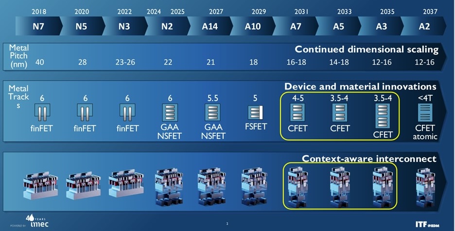
In addition to the chip makers’ GAA presentations, Samsung, CEA Leti, and Imec also presented on CFET or stacked FET transistors which is in line to be the next phase of transistors. CFETs are scheduled to see introduction in 2031 according to the imec roadmap, which is now the generally accepted technology roadmap for the industry. While finFET transistors were skyscrapers compared to planer transistors. The GAA transistors require new process technology to create the structures. As the industry moves to GAA the semiconductor industry has moved into a new era of 3D integration (Figure 1)


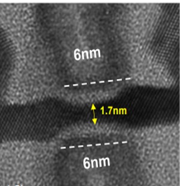
The IEDM 2024 publicity information states that the TSMC presentation featured the most advanced logic technology at this IEDM meeting. The SRAM density is approximately 38Mb/mm2. During his short course, Victor Moroz of Synopsys discussed that we are approaching the end of channel shrinking, so transistor shrinking will be slowing. 2D materials were expected to increase the speed of the transistor, but these materials still need work on integration, and at the moment, according to Moroz, not yet performing as well as silicon. Intel’s talk demonstrated a 6nm gate length, which enables a bit more shrinkage in the transistor (Figure 2). Previously 10nm was thought to be the lower limit.
This inability to scale the transistor is pushing 3D packaging to the forefront of semiconductor technology to get the performance it needs for next-generation computing. 3D packaging processes are becoming more complex and had several sessions at IEDM 2024.
Session 21 included eight papers on the challenges and future of 3D packaging with all the major 3D semiconductor players presenting: Nvidia, Qualcomm, and AMD. The industry is moving from 2.5D to 3D, and now 3.5D and 9x reticle packaging technology is moving to the forefront of semiconductor process and layout technology.
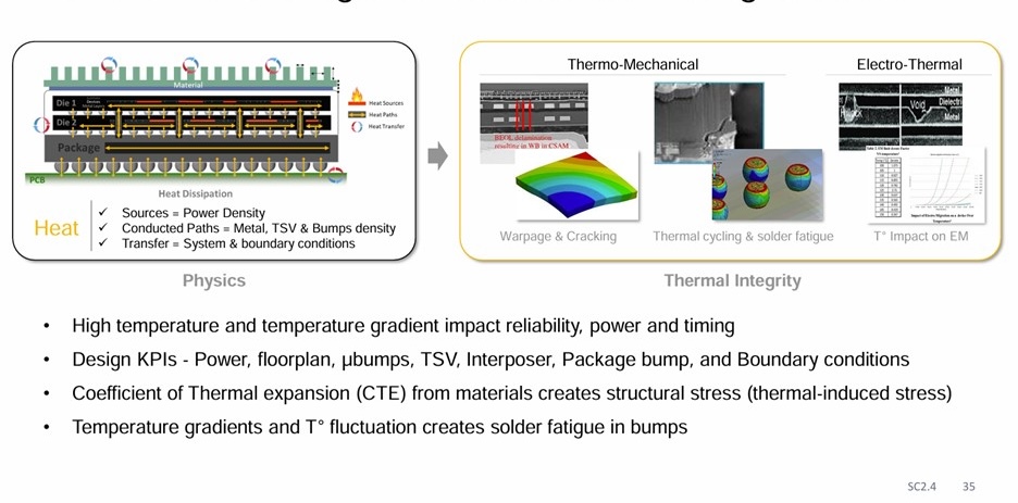
System Technology Co-Optimization (STCO), is an acronym that was thrown around a great deal at IEDM and other conferences. Packaging multiple dice together is a complicated proposition (Figure 3). The first thought is what type of functionality do I want to achieve, followed by power, performance, and area. Then you add in cost and thermal factors along with power, heat, and stress. The cost to put the system together is also a factor, but at the moment it looks like the AI world is willing to pay a steep price to train their models, leaving the cost consideration for the automakers and other chiplet applications.

There was also some mention of 3D packaging reducing the power needed, as well as the new chiplet systems reducing the time required to train models. There is a power versus training time versus cost consideration that will start to become important in the near future.
Chiplets Entice Front-end Equipment Makers
The rise of chiplets has caught the attention of the semiconductor equipment industry. In the past, companies that worked on the silicon side of the business didn’t pay much attention to the packaging side of the business. As chiplets use wafer-level processing, and the need for smaller pitches to create smaller form factors and faster systems grows, the silicon equipment companies are moving into the chiplet process space.
Applied Materials held a panel discussion moderated by Ian Cutress of More than Moore. Panelists included Terrence Lee of Applied Materials, Johanna Swan of Intel, Deepak Kulkarni of AMD, and Kam Kittrell of Cadence (feature image). They covered many of the pertinent topics of 3D packaging. Mapping out standards, design optimization, adapting for photonics, power efficiencies, system timing, and panel process were a few of the highlights.
Chiplets for the Masses
Based upon presentations and conversations at IEDM, chiplets are getting to mainstream. Currently, most applications and systems are focused on high-performance computing for AI. Systems for automotive are picking up momentum as well.
Bob Patti of NHanced Semiconductor Inc. pointed out that in these chiplet systems, the chips or tiles are typically made by one chip manufacturer and that chip manufacturer then assembles the tiles into the chiplet. These services are typically performed for the big AI vendors such as Nvidia, or AMD. Smaller companies are out of luck! This is where the OSATS such as NHanced Semiconductor come into play. Companies can assemble their best-of-breed chipset or tiles, and will be able to get them assembled into the desired chiplet, thus helping to level the playing field for the entire electronics industry. The transition from planer chips to 3D packaging has been coming for a long time. It looks like we will now see it accelerated at a rapid pace.


