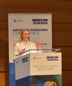
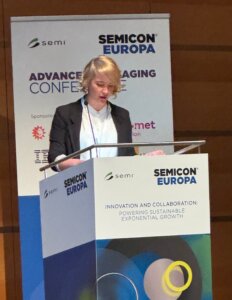
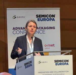
Now that imec’s Luc Van den hove declared advanced packaging is key to the advancement of semiconductors, everyone in the industry needs to catch up to those who have been following the course of these technologies while they were in development. The Advanced Packaging Conference (APC) at SEMICON Europa 2024 was a good place to do that. And our community members were there to lend a hand.
Many presentations offered historical overviews of advanced packaging. So wherever you are in your understanding of advanced packaging, the context was provided to catch you up to where we are today. If you missed the APC this year, you might want to check it out next year. Unfortunately, I didn’t catch the entire line-up, but here are highlights from the morning session.
Advanced Packaging for Power-hungry AI
If, like me, you’re concerned about the amount of power generative AI gobbles up, Mark Gerber of ASE Group explained how advanced packaging technologies will improve power efficiencies in semiconductor devices.
IBM’s James Sexton explained how chiplet architectures can address the power challenge created by AI foundation models for large scale computing. Many domains have unlabeled data that can be used to train custom foundation models. This is creating a paradigm shift where we need to move the compute to the data.

“Sustainable progress needs transformation of hardware and software,” said Sexton. IBM plans to build a chiplet ecosystem for enterprise computing to address the power challenges of foundational AI.
According to Amkor’s YoungDo Kweon, the power drain on data centers has more to do with do with power in-and-out. The challenge is the power distribution network (PDN) and thermal dissipation (TD) path as data center packages become larger and more complex with multi dies and dense interconnect. Heterogeneously integrated, chiplet-based packaging improves both PDN and TD, he said.
Anne Jourdain of imec declared that hybrid bonding is the technology of choice for 3D interconnect technology. She explained the basics of hybrid bonding and then shared why SiCN dielectric material improves the Cu-Cu connections, making it possible to scale to finer pitch. In wafer-to-wafer hybrid bonding, she said imec researchers have achieved 400nm pitch and is working toward 100nm pitch.

SiCN dielectric can also be applied to die-to-wafer approaches, explained Jourdain, but there is added complexity due to the possible presence of particles as a result of wafer dicing. Plasma dicing solves many of these challenges. While laser dicing leaves a residue, plasma process do not.
Dr. Jessica Stubbe, of MKS Atotech, explained how material science can impact the structure microbumps, which, along with through silicon vias (TSVs) are critical part of the 3D IC interconnect.
Stubbe explained that chip designs require fine-pitch bump applications to meet the need need for higher I/O density. Copper electrolytes make it possible to reduce pitch sizes by addressing the current mechanical challenge of miniaturizing micro bumps. These advanced electrolytes are tailor made according to the design of ECD additives. This makes it possible to meet coplanarity criteria, she explained. Coplanarity among the micro bumps is critical to make sure there are no shorts or opens in the interconnect array.

Providing the equipment perspective, Elisabeth Brandl, EV Group, described different approaches for 2.5D packaging, comparing the advantages/challenges of Si interposers. She said using silicon bridge dies for chiplet integration provides similar bandwidth of silicon in a reduced area and can achieve fine pitches. This could be a cost advantage. Conversely, organic interposers create thermal management issues and I/O density limitations.
A Word on Panel Level Packaging
In addition to our member presentations at APC, I caught a few moments to talk about panel level packaging with Sally Ann Henry and Jim Straus, of our member company ACM Research.
In response for the growing demand of panel-level packaging solutions for both organic and glass panels, the company just introduced three new tools. These include an electrochemical plating tool, a bevel cleaning too, and a vacuum flux remover. The electrochemical plating tool, which supports 500x500mm and 600x600mm panels, uses a horizontal, rotating method for uniform film deposition. The vacuum flux remover addresses solder ball issues by rinsing with water and IPA followed by a vacuum to remove residuals. These adaptations leverage existing wafer-level processes, driven by the demand for AI and HPC chips, which benefit from high-density panel packaging.
To learn more about what our members were showcasing at SEMICON Europa, be sure to tune into this week’s Member Spotlight Podcast.


