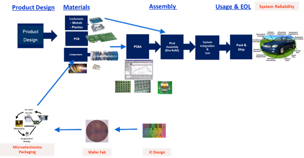
Semiconductor packaging is a complex and evolving field, involving multiple disciplines. As a microelectronics packaging engineer, I focus on the “interconnect thread” from the chip to the system (Figure 1).

To me, packaging is about interconnectivity (essentially). The primary function of packaging is to provide the interconnection from the IC to the system, for signal distribution and power distribution. What makes it more complex (and thus interesting) is the enabling functions, including mechanical reliability (especially under complex loading conditions in diverse use environments – thus various failure modes and mechanisms); thermal dissipation (especially important for high power and also due to the multiple interfaces in the system); as well as manufacturability that has to be considered (such as low temperature soldering, fine pitch processes, cost and quality, and very importantly, sustainability). These electro-mechano-thermal functions of the interconnect are what makes “packaging” such a critical area for semiconductor technology today. In the age of heterogeneous integration, a variety of interconnects in the same package have to be considered.
From the die to the package and to the system, there are many forms of interconnects. At the package level, there are RDL (redistribution layer), TSV (through silicon via), EMIB, wire bonding and flip chip, etc. Solder interconnects, in the form of solder joints, solder bumps (and copper pillars), BGA balls and so on, are a very important form of interconnects. Today, there is also direct copper connection (without solder) for the finest pitch applications. Other forms of interconnects include component terminations (such as leads, balls and pads). Photonics is emerging as a very important form of interconnects (including wave guides, optical RDL, optical TSV, …) Then, there are various forms of interconnects at the PCB level and the system level, such as connectors, fiber, cables, etc. These various forms of interconnects together fulfil the functions of packaging, from the chip to the system.
Packaging has evolved in complexity and capability. If we look at the evolution over the past several decades, the overriding trend is that interconnects are becoming shorter (per I/O) – “Less is Moore”, as short interconnects can give better electrical performance, lower power consumption, smaller areas and often lower cost, and hopefully better reliability and sustainability as well, even though the total length of interconnects in a device have become longer (due to package complexity for heterogeneous integration).
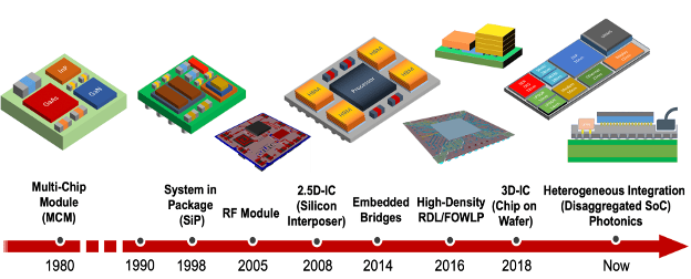
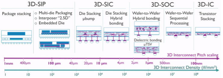
Over the years, packaging has evolved from 2D to 2.5D/3D, from single chip packages to multi-chip SiPs for heterogeneous integration (Figure 2), with an overall trend towards higher density (Figure 3), finer pitch (“scale down”), in larger packages (“scale out”) and in 3D heterogeneous packages. Today with hybrid bonding, the interconnect pitch scales down to 1µm (and below), while the density increases to 1 million I/Os (and higher) per mm2, interconnecting billions of transistors.


The Importance of Interconnect Reliability

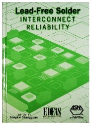
For semiconductor devices to perform their functions in the field, reliability is essential. Packaging reliability is really about interconnect reliability – including mechanical reliability, electrical reliability (such as electromigration – especially as the current density increases with finer interconnects), electrochemical reliability (such as surface insulation resistance, or SIR), and signal integrity (especially for high frequency applications). More details can be found in my book “Lead-Free Solder Interconnect Reliability” (Figure 4). It was noted (in my publications as well as others’), as early as several decades ago, that the Sn-Ag-Cu based solder alloys may not perform adequately under harsh environmental conditions and could fail even earlier than the Sn-Pb solder alloy under such conditions. This has led to the development of alternative (“high reliability”) lead-free solder alloys for automotive electronics and other similar applications.
It is worth noting that miniaturization is exacerbating the many reliability issues that have existed for interconnects. For example, smaller solder interconnects are more susceptible to thermomechanical failures. Finer pitch interconnects – with a higher current density – are more prone to electromigration, especially so for Bi-containing alloys. Tighter spacings between solder interconnects make them more vulnerable to failures such as whiskering, α particle emission, and solder extrusion during thermal cycling, etc. As the solder volume decreases for finer interconnects, interfacial IMC’s (intermetallic compounds) play a greater role in interconnect reliability. Interfacial thermal resistance also becomes more important in thermal dissipation. Miniaturized solder interconnects are also more susceptible to defects (such as voiding, bridging, etc.) Tightly spaced interconnects can also play a role in electrical integrity such as cross talk.
Increasingly, thermal integrity is becoming a more important issue, and innovative thermal interface materials (TIM) have evolved, such as liquid metal, sintered nano-Ag/Cu, etc. Thermal Test Chips (TTC) have become an essential tool for thermal characterization.
Interconnect materials also play a critical role in sustainability. Low temperature solders, ultra-low residue no-clean fluxes, are some of the recent examples of how innovations in interconnect materials can contribute to sustainability. It has also been noted recently that the life cycle emissions associated with Cu are orders of magnitude lower than Ag; this could play a role in considering the use of sintered nano-Cu and nano-Ag in power electronics.
For cryogenic electronics for superconducting quantum computing, interconnect reliability below -150° C is essential.
For flexible hybrid electronics (FHE), a new set of interconnect materials have been developed to meet different performance and reliability expectations, such as stretchability, bendability, and so on.
Hybrid bonding has emerged as the most advanced method for fine pitch interconnects through direct copper connection, and has become an essential enabler for chiplets and 3DIC. Hybrid bonding not only enables the finest interconnect pitch, but also enables superior reliability (such as high temperature storage and temperature cycling – due to the absence of defects such as voiding and intermetallics growth associated with the presence of solder, and oxidation and corrosion resistance as the Cu interconnects are encapsulated by the surrounding dielectrics.) Direct copper interconnection also helps reduce thermal resistance and electrical parasitic capacitance, thereby improving thermal integrity and signal integrity. This interconnect technique is a critical enabler for the use of chiplets in various fabrics.

The success of hybrid bonding in high volume production depends on the process maturity and the support of the eco-system, including materials and equipment. These important aspects have been presented in my recent book “Director Copper Interconnection for Advanced Semiconductor Technology” (Figure. 5). Further discussions will take place at the inaugural IEEE Hybrid Bonding Symposium (HBS) .
Overall, following the “interconnector thread” gives us the pathway on the technology trend for semiconductor packaging and heterogeneous integration, and points to directions for new innovations that are needed to enable further advancements – in2.5D/3D, high frequency devices, flexible electronics, cryogenic electronics, and large form factor systems with high reliability, signal integrity, power and thermal integrity.
Newer form interconnects, from known good die to known good system, will enable further innovations in semiconductor packaging in the years to come.
For further information, please contact dksg@ieee.org.


