How A Collaborative Partnership Is Accelerating PLP Innovation
Panel-level advanced packaging technologies have been in development for more than a decade. They began as a way to reduce costs and improve yields for fan-out wafer-level applications. Smartphone applications – particularly fingerprint sensors – promised the volumes that would make the investment successful.
However, memories of the fiasco of 450mm wafer efforts lived in the minds of many. Why make the investment in an ecosystem that may not demand high enough volumes to insure return on investment? Still, there were those who believed in the promise of panel-level packaging. Development efforts persevered, and PLP has moved through R&D and into pilot production. Still, through it all, many remained skeptical about there being high enough volumes to support it.
The Era of AI, coupled with the emergence of glass substrates, is set to change all that.
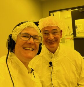
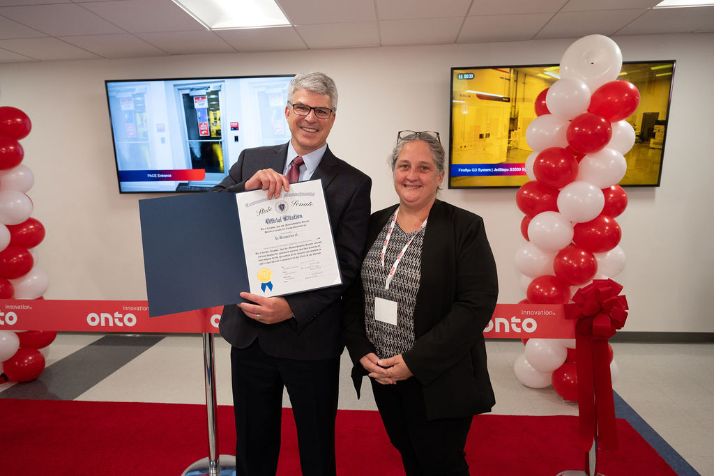
On September 30, 2024, I visited Onto Innovation’s headquarters in Wilmington, MA to attend the grand opening of its Packaging Applications Center of Excellence (PACE). The company has partnered with like-minded suppliers of the PLP ecosystem to accelerate the development of PLP technologies for both organic and glass substrates. These include 3D InCites Members: LPKF Laser & Electronics, Evatec, MKS-Atotech and Lam Research; as well as Resonac, Corning, and others.
I spoke with CEO Mike Plisinski, and toured the PACE facility with its director Keith Best. I also connected with attendees from LPKF, Corning, Evatec, MKS Atotech, and Resonac to learn more about PACE’s mission. Lastly, I spoke with Dave Robertson, Massachusetts State Representative for Wilmington and nearby Tewksbury about the support the State of Massachusetts gives to the microelectronics sector.
What’s Driving Panel – level Advanced Packaging?
“The ERA of AI is the most transformative era in our lifetime,” said Plisinksi. “It has the potential to be as transformative as electricity or the Internet,” echoing what Jamie Dimon, the CEO of JPMorgan Chase, conveyed in his annual shareholder letter earlier this year. He added that it goes far beyond revenue growth for the semiconductor industry. It’s the impact AI will have on society and the issues it can solve.
Over the past year, demand for AI chips has increased dramatically, driven by generative AI applications. One company, Nvidia, is emerging as the “King of the Industry”, and its efforts to increase processing power has led them away from the latest generation of front-end transistor technology.
“Nvidia leveraged advanced packaging to provide the processing and compute power necessary to unlock those AI algorithms,” noted Plisinski. Specifically, Nvidia combined 2.5D and 3D memory stacking to reduce interconnect distances and improve power efficiency, device performance,area and cost (PPAC) of the device.
While initially, these implementations have been in wafer format, as AI chipsets increase in size, moving to panel format makes sense to increase yield and reduce waste. It’s the basic square-peg/round hole dilemma.
One of the current challenges that the industry hopes will be solved with glass core substrates, is that silicon is not available in panel format. To achieve the high densities equivalent to that of silicon wafers means reducing line/space dimensions of redistribution layers (RDL) on both fan-out and interposer packages. Glass core substrates will also allow for finer features.
Enter the Packaging Application Center of Excellence

Keith Best, Director of PACE, took me on a tour of the facility, which is equipped with Onto Innovation’s lithography and inspection tools, a process lab, and software that connects data from Onto and third-party tools to provide insightful and actionable analytics and dashboards. He provided a step-by-step description of the processes as panels move from the photoresist coater, to the lithography stepper, to the developer, and then to the inspection system.
Best said Onto Innovation decided to focus efforts in PACE on PLP because package sizes are growing to 100mm and beyond. “Customers are talking about package sizes of 150mm, which means that wafers will no longer be relevant in this space, and packages need to be built on panels.”
The collaboration partners are part of a virtual line. Lithography processes happen at PACE, and the panels are shipped to, for example, Evatec for seed metal deposition and Lam Research for electroplating, and then back to PACE for inspection.
“Everyone in the collaboration will benefit by having access to next-generation chemistry, as well as next-generation lithography. Because you can’t plate 2-micron line/space unless you have an advanced packaging lithography tool,” said Best.
Collaboration partners came together through conversations at events such as IMAPS DPC, with “adjacent OEMS who had the same mindset we had,” said Best. There is no fee to be part of PACE at the moment. Rather each one of the partners will have a statement of work with Onto Innovation, specific to the processes and/or materials they provide. By providing the “bookend” capabilities – leading edge lithography for sub-2-micron line/space, and then post-process inspection, Onto is making it possible to optimize panel level packaging processes.
“We have the capability now to print wide field large packages that aren’t coming to market for several years at 1-micron capabilities. For companies that wanted to invest in and see how their plating or chemistries perform with these more advanced structures, they had no way to test,” said Plisinksi.
He explained that PACE gives Onto Innovation the opportunity to leverage its equipment, to print and image these structures and see how the plating adhesion works on glass. Furthermore, he added, the process control capabilities of the Firefly system make it possible for customers to learn and develop and characterize their process equipment and use Onto’s software to connect all the pieces together.
Why Join PACE?
Ralph Zoberbier, CMO of Evatec, said that being part of PACE gives the company a step forward as a viable supply chain partner. It also gives Evatec engineers the opportunity to gain experience and know-how while working with engineers at other companies. “We also want to enhance our products and are working on new generation panel PVD type of technologies,” he added.
“Many semiconductor industry innovations occur at the intersection of materials and process equipment,” noted Junro Yoon, of Corning Advanced Optics. “We are excited by this partnership to uncover new innovations.”
“As we move into the next generation of advanced packaging, it’s clear that no one company is an expert on all the different areas,” said Kuldip Jopal, MKS-Atotech. For MKS-Atotech, that translates to support in developing next generation dielectric materials, and also collaboration on developing test vehicles to address finer pitch. Collaboration with Onto Innovation in PACE does that by gaining access to lithography and inspection tools that help in pre- and post- creation of fine lines and spaces.”
Richard Noack, LPKF, noted that joining PACE gave the company the opportunity to participate in an entire ecosystem focused on glass packaging. LPKF provides the laser induced glass etch process to form through glass vias.
Continuing the “Mass Miracle”
Dave Robertson, Massachusetts State Representative for Wilmington and nearby Tewksbury MA, also attended the Grand Opening. We talked about the advantages of building technology businesses in Massachusetts. He reminisced about the 90’s initiative dubbed “The Mass Miracle” when the northeast corridor became a technology hub, with companies like Cisco, Digital Equipment Corp, Wang Computers, Sun Microsystems, and others fueling demand for computer chips; and companies like Analog Devices designing them.
Recalling Massachusetts strength in the industrial era, followed by a slump of offshoring, Robertson said the state’s continued investment in technology makes it a great place for high tech companies to set up shop. He also highlighted the education opportunities from K-12, noting that the state ranks among the top in the nation for education. He also talked about free community college for people over 25 who want to seek new workforce opportunities. On the downside, the region is plagued by a high cost of living, due to expensive housing and utilities. He said he hopes that with more company’s like Onto Innovation coming in, that will help with costs.

What’s Next for PACE?
While immediate efforts will focus on bringing PLP on organic and glass substrates to high volume to support the growth in AI, the partners don’t plan to stop there.
As customers clamor for even finer line/spaces down to 1 micron, Best says they will need to consider other potential partners to support CMP, which currently is only in development for PLP.
Companies who are interested in joining PACE should reach out to pace@ontoinnovation.com.
To hear all the interviews from the PACE Grand Opening, be sure to listen to the podcast episode.


