


Call me crazy, but after spending three days at the 2024 International Microelectronics and Packaging Society (IMAPS) Symposium in Boston learning about the latest industry trends and technology advancements, I think it’s time for the entire advanced packaging world to fully adopt the concepts of “Interconnectology” and “Interconnectologist”.
The inspiration came when I read a LinkedIn post from Eelco Bergman, of our member company, Saras Micro Devices:
“Beautiful morning in Boston. Ready for the start of #IMAPS2024 Symposium. Should be a great week for interconnectologists interested in the latest developments in advanced packaging. Stop by Saras Microdevices at booth 502 to learn how we’re improving power delivery with STile.”
Clearly, Eelco’s been paying attention to what we’ve been doing with Jillian Carapella’s new blog, Interconnectology 101. It features interviews with our premium members to educate newcomers to the industry. He also may have heard the podcast episode with Simon McElrea, “So you Want To Be an Interconnectologist?”
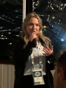
IMAPS International Symposium 2024 drew more than 900 attendees – aspiring interconnectologists all – and 95 exhibitors to Boston. The crowd of attendees continue to be younger and more diverse each year. For the second year running, the Steve Adamson Award went to a women Ph.D. student from SUNY Binghamton, Emma Pawliczak.
As last year’s Steve Adamson Award Winner, Nicole Wongk said to me, we will know we’re at 50% women when there’s a line in the woman’s restroom! I still remember the days when the women’s restroom was virtually empty and there was no casual chatting like that over the sinks.
But I digress. Let me explain why I think we should be calling ourselves interconnectologists.
Scale Down and Scale Out

Dev Palmer, who recently took over the leadership of the National Advanced Packaging Manufacturing Program (NAPMP) from Dr. Subu Iyer, updated us on the program as CHIPS Acts funds begin being disbursed. Iyer is still involved, as the Technical Director.
He described Iyer’s work setting the stage as the composer. He, Palmer, is the arranger. And the rest of the industry is “the band.”
Palmer introduced the concept of scaling down (miniaturization) and scaling out (accelerating packaging system integration) as the misson of the National Advanced Packaging Manufacturing Program (NAPMP).
Scaling down involves accelerating the convergence of fabrication and packaging by miniaturizing features on packages. Scaling out focuses on creating packages that accommodate a larger number of closely packed, heterogeneous chiplets and addressing power, heat dissipation, and connectivity standards.
Palmer explained that the NAPMP’s advanced packaging piloting facility (APPF) is a key component of this strategy, with a focus on packaging advanced chips in the US.
He also reiterated what we’ve been hearing industry wide: that collaboration among various stakeholders, including commercial companies, academia, and government agencies, is crucial for success.
In my opinion, all of this accurately captures the concept of Inteconnectology.
More Focus on Interconnect, Less on Package

Beth Keser, of ZeroASIC, talked about the shift from monolithic chips to chiplets to improve cost and efficiency. She highlighted the challenges of Moore’s law and increasing silicon costs, advocating for chiplets to reduce unit costs and improve yield.
Keser emphasized the need to improve chiplet-to-chiplet interconnect processes, rather than the off-package interconnect to meet this performance. She explained that transistor innovation, interconnect advancement, and design technology co-optimization are all needed to match the performance of monolithic SoCs at a lower cost.
“A lot of the advanced packaging topics that you’ve heard about this week are not cheap, tiny packages that you can get for less than $1.” said Keser. “They’re very expensive package types, and we have to design them very well and choose them with very good care to make sure that your overall product costs still benefits from chiplets.”
As a start-up, Keser explained that Zero ASIC’s goal is to democratize access to the most advanced node technology. To achieve its goal, the fabless company aims to become the “Amazon for ASICs”. They break up IP into a vast library of chiplets that can be interconnected on an active base she called “EFABRIC” via a standard interface, such as the Universal Chiplet Interconnect Express – or UCIe.
What Zero ASIC is doing doesn’t sound like a job for just any old packaging engineer. It calls for interconnectologists!
Advanced Packaging, or Interconnectology?

Lightmatter’s Nick Harris highlighted the exponential growth in AI and supercomputing. He said current supercomputers use 100,000 GPUs, with costs split 70% for compute and 30% for networking. Thanks to AI, he said, what was once a niche field is now a critical component for big tech companies like Google, Microsoft, Amazon, and Meta.
Lightmatter’s technology aims to improve interconnect efficiency, using 256 optical fibers for flatter networking. The company has developed a chip with a million photonic components, showcasing significant progress in integrating photonics with advanced packaging.
When we’re integrated photonics into the device, is it still advanced packaging? Or is it interconnectology?
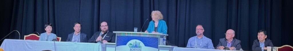
Ou Li, ASE; S.P. Jeng, Consultant, TSMC; Craig Bishop, Deca; Jan Vadraman, Techsearch International; Brett Wilkerson, AMD; Satoru ; and Mike Kelly, Amkor; Kuramochi, DNP
Jan Vardaman’s traditional Wednesday night panel focused on the advantages and challenges of Redistribution Layer (RDL) technologies versus traditional silicon interposers. Key points included RDL’s cost-effectiveness, flexibility, and compatibility with various applications, such as mobile, automotive, and high-performance computing. Panelists shared concerns about signal integrity, copper migration, and the feasibility of large panels. They also highlighted metrology challenges, including warpage and uniformity issues.
The conversation also covered the benefits of bridge solutions, which enhance yield and reduce routing layers. The panelists agreed on the economic drivers for adopting RDL and the need for advanced equipment and processes to address these challenges.
So is this advanced packaging or advanced interconnectology?
Bottom line: These days it’s less about the packaging of the chip, and more about the interconnect. So why are we still calling it advanced packaging?
Isn’t i cooler and sexier to tell people that you’re an interconnectologist working on advanced Interconnectology, than saying you’re an advanced packaging engineer. It also better describes the technologies that are needed to support today’s high performance computing applications.
For more from the IMAPS International Symposium, be sure to follow the 3D InCites Podcast. We’ve got lots more to come in the next few episodes from the keynoters, winners of this year’s Society Awards, some panelists, and the 3D InCites members who participated. These episodes will take a deeper dive into the key topics of this year’s event, in the interconnectologists’ own words.


