


(2nm semiconductor manufacturing foundries)
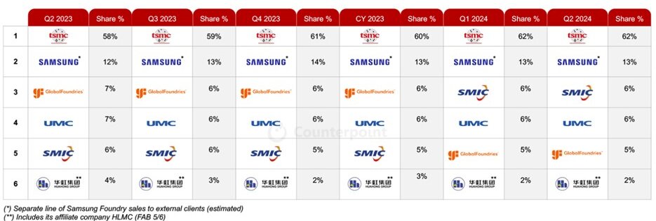
UMC started the semiconductor manufacturing foundry business in 1980, followed a few years later by TSMC. You could say the rest is history. TSMC has come to dominate the foundry industry for wafer processing and advanced packaging. TSMC has a 62% market share in the second quarter of 2024 on revenues of $20.82 billion (Figure 1). However, new competition is emerging at 2nm so will the landscape change?
A considerable part of TSMC’s success and high revenue numbers results from TSMC being the dominant game in town when it comes to manufacturing semiconductors below the 5nm node. TSMC committed to double patterning and then was the first to use EUV lithography; other foundries slowed their technology shrinks at double patterning.
According to different news reports TSMC has approximately 200,000 wafer starts per month running at 5nm and below, supplying chips to Apple, AMD, Nvidia, and Intel. TSMC has also taken the lead in advanced packaging providing 2.5 and 3D packaging to its customers. The Chip on Wafer on Substrate (CoWoS) 3DFabric package size is up to 1700 mm² or 2x reticle size and is used for customers with large AI chips using high bandwidth memory. TSMC is currently capacity-constrained and is looking for 40k wspm capacity by the end of 2024 and to have balanced capacity in 2025 possibly moving to large glass substrates using flat panel display technology.
TSMC is the dominant semiconductor foundry and has the most wafers available for production below 5nm; however, the competition for business below 5nm is emerging, and as the new fabs come online, the question is: Will TSMC lose market share as the competition heats up in the next few years?
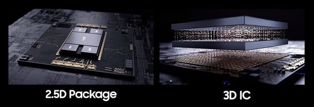
Samsung has been competing in the foundry space since 2005 and has a 13% market share on average. Samsung is TSMC’s primary competitor at the leading edge and occasionally introduces technology ahead of TSMC. Samsung was the first foundry to introduce gate-all-around (GAA) technology in production. Some of this advanced capability comes from a relationship with IBM, which uses Samsung as a foundry to produce advanced chips such as the new Teleum II ASIC processor that will drive IBM’s mainframes. Samsung has 2.5 and 3D packaging technologies known as the X-cube and is introducing a new 3D technology called SAINT (Samsung Advanced Interconnect Technology) platform for HBM4. Samsung is also working on panel-level packaging (Figure 2).
Rapidus is the newest 2nm semiconductor manufacturing foundry looking to manufacture and package chips at the 2nm process node. Rapidus is expected to start pilot production in 2025 on 2nm technology supported by IBM and IMEC, with full production starting in 2027. Rapidus is also partnering with IBM for chiplet packaging technology for 2nm node chips, so it will be able to offer turnkey chip manufacturing for its customers.
Another difference between Rapidus and its competitors is that Rapidus will try to use single-wafer process technology to improve cycle time. Rapidus is working closely with leading-edge equipment manufacturers to modify the equipment so a single wafer can move through the factory at a time.
Semiconductors are traditionally processed in what is referred to as batch processing: 25 wafers to a FOUP, and 50 wafers in one lot. Advanced process equipment has evolved to single-wafer processing with multiple process chambers on each tool, or a sequence of process chambers to get the desired result. The batch process can take as long as 3 months to process a lot wafers, and then package them. There is also the challenge in the foundry that a customer’s order can be less than 25 wafers. This can create inefficiencies in the foundry and increase the cost of the chip. Rapidus thinks that by using single wafer processing the cycle time can be reduced significantly, and fab efficiency and costs will be improved. Rapidus will focus primarily on the Japanese market, but its first announced customer is Tenstorrent out of Canada using a RISC-V design.
Last but not least is Intel. Intel announced its IDM 2.0 in 2021 describing how it would reboot its manufacturing capabilities and provide leading-edge transistor and packaging technology to the semiconductor industry. As part of IDM 2.0 Intel is offering both silicon and packaging foundry services to the industry.
Intel’s chip design operations have a choice to either use Intel, or other foundries to manufacture wafers. Intel’s 3nm process technology is being offered to its customers along with Intel’s version of 2.5 and 3D packaging of EMIB and Foveros (Figure 3). Intel has also announced panel-level packaging plans.
While Intel is offering 3nm technology to its customers, it is using TSMC for some 3nm products. One of Intel’s major differentiations in the foundry packaging space is that, according to Daniel Nenni of SemiWiki, Intel is the only foundry that will package chiplets that they do not manufacture in-house. It is too early to tell if this will be a competitive advantage, or if it will re-shore a significant amount of packaging to the United States.
Pat Gelsinger announced significant business for the Intel Foundry including Microsoft, and the ability for customers to start taping out at the 18n node. The flip side is Intel has also announced that the foundry business will not be profitable until the 2030 time-frame, raising some financial concerns.
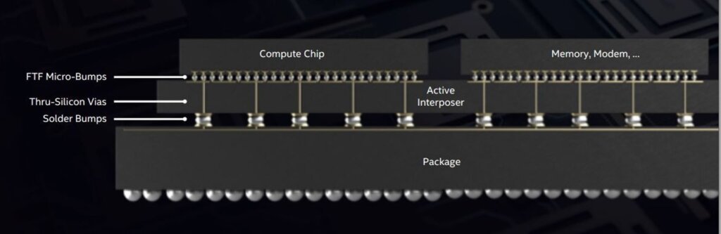
Figure 3 Intel FOVEROS packaging technology. Source Intel
So now there are four foundries that in 2027 will give the industry four different foundry opportunities at 2nm and for chiplet technology. OSATS are also gearing up their chiplet operations, which has the potential to make chiplet costs very competitive. Most of the packaging industry is looking at a variation of CoWoS using glass panels to support the large chips used for AI to improve yields and reduce costs. Rapidus, Samsung, and Intel are all ramping up technology and manufacturing capability to compete with TSMC and Samsung at 2nm. Will there be enough 2nm and advanced packaging business for Intel and Rapidus to become profitable in the foundry business, and to make a dent in TSMC’s market share leadership?


