


By Jim Straus and Sally-Ann Henry, ACM Research
While heterogeneous integration of multiple components and 2.5D/3D packaging techniques pair perfectly with complex stacking architectures, these technologies elicit high demands on device manufacturing processes. Through-silicon vias (TSVs) are a key enabler, allowing direct chip-to-chip connection through the chip stack without requiring wire bonding or edge wiring.
The growing demand for miniaturized semiconductor chips and their applications in different sectors such as telecommunications, automotive, aerospace and defense, and consumer electronic devices, etc., is accelerating the growth of the TSV technology market globally. TSV technology allows state-of-the-art packages to increase packaging density and deliver high performance and low power consumption.
However, optimizing TSV processes relies on a broad set of technologies. This article provides insight into ACM Research’s propriety solutions, illustrating its role and importance to TSV processing and explaining the benefits. First, the focus is on TSV cleaning using ACM Research’s SAPS™ megasonic technology.
TSV Process Overview
Before delving into TSV cleaning, it’s important to understand what is involved in the TSV process (see Figure 1) including the cleaning challenges it creates. Typically, the TSV goes through the etching process through the silicon substrate to create cavities, and then fill them with a conductive material, such as copper or tungsten, to form a vertical electrical connection.

The required TSV size depends on the application. The reactive ion etching (RIE) process, such as the Bosch process, is commonly used to fabricate deep vias due to its ability to produce features with vertical sidewalls and high aspect ratio. However, forming these vias with smooth sidewalls is challenging, and the RIE process typically results in the formation of numerous polymer residuals at the bottom and sidewall of vias.
Removing these fluorocarbon polymers and optimizing the TSV requires a reliable cleaning process, after which the via is filled – typically with copper – to make the interconnect between different layers in the 3D stack. This is achieved by electrochemical plating (ECP), followed by the last of these steps, polishing. ACM Research’s proprietary stress-free polishing (SFP) technology affords some unique advantages over other polishing offerings, which will be addressed in part three of this series.
Megasonic TSV Cleaning
Megasonic cleaning uses sound waves traveling through a liquid to produce cavitation – rapid formation and collapse of vapor bubbles within the liquid. Megasonic cleaning’s high-frequency sound waves result in controlled cavitation that gently removes sidewall polymers and residue. By creating a much thinner boundary layer, megasonic cleaning makes chemicals less viscous, enabling them to reach the bottom of vias. This is vital, as incomplete cleaning deteriorates device performance. Particles and residue left in the holes result in low breakdown voltage, high leakage current, and low yield.
ACM Research’s Space Alternated Phase Shift (SAPS™) technology takes megasonics a step further, outperforming conventional megasonic cleaning products and exceeding expectations beyond removing random defects (Figure 2). Unlike the stationary megasonic transducers used in previous generations of megasonic wafer cleaning systems, SAPS technology moves or tilts the transducer while the wafer rotates, enabling megasonic energy to be delivered uniformly across all points on the wafer, regardless of wafer flatness or uniformity.
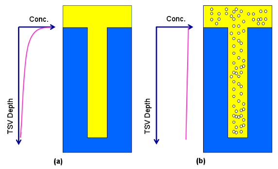
On a microscopic level, megasonic energy can reach every point on the wafer surface, removing random defects much more effectively and completely than conventional megasonic or jet spray processes. SAPS technology provides uniform megasonic energy distribution to the wafer surface and demonstrates a clear capability for removing residue at the bottom of vias, as shown in Figure 3.
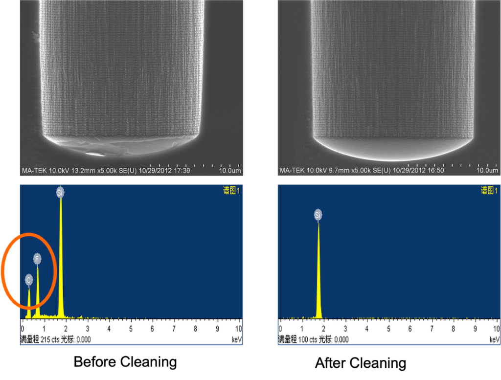
The results show that SAPS megasonic technology delivers high cleaning efficiency for fluoropolymer sidewall residue removal in post-silicon-etch TSV cleaning processes, yielding minimal damage to the structures and low material loss.
![[err-ad-fallback-title]](http://www.3dincites.com/wp-content/plugins/a3-lazy-load/assets/images/lazy_placeholder.gif)
Now that you have formed TSVs and cleaned them efficiently, these need to be plated using a metal appropriate to the device application. ACM Research’s ECP technology helps ensure your final product’s desired quality and electrical performance.
Electroplating of Metal for TSV Formation
The SAPS™ megasonic technology developed by ACM Research enables chipmakers to remove residue following TSV formation much more effectively and completely than other megasonic or jet spray processes. In part two, we turn to electroplating.
Electroplating is an essential process in TSV fabrication. Once the vias have been thoroughly cleaned, and conformal linear and seed layers have been deposited, they are subsequently filled with electroplating of metal, typically copper. Void-free electroplating of Cu in high-aspect-ratio features is vital to deliver low resistivity and high reliability for transistor performance. However, void-free fill and uniform deposition at a high plating rate are challenging to achieve with conventional deposition tools. Mass transport limitation reduces the deposition rate, and results in voids in the vias and uneven Cu surface. ACM Research’s Ultra ECP system has expertise in integrating the optimal Cu plating into the TSV formation process.
Ultra ECP for WLP
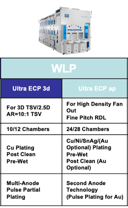
ACM Research’s Ultra ECP platform includes two systems that target wafer-level packaging: Ultra ECP ap and Ultra ECP 3d (see Figure 1). Ultra ECP ap system supports Cu via filling and Cu pillar bumping for Cu, it delivers high-speed plating technology for uniform deposition in vias without sacrificing the plating rate. Ultra ECP 3d is integrated with ACM Research’s exclusive Multi-Anode Partial Plating function, which allows the deposition of Cu metal layer on via structures of 3D TSVs and 2.5D interposers and is compatible with aspect ratios of 10:1 and beyond.
Second-anode design
Traditionally, electroplating systems utilize a single anode, limiting the deposition rate and uniformity across the wafer surface. The addition of a second anode in the Ultra ECP platform enables precise control over current distribution during the electroplating process, minimizing variations in plating thickness and improving overall uniformity. This innovation results in more consistent deposition rates and better quality of plated layers, leading to higher yields and improved device performance as well as better process times and throughputs.
Additional Benefits
The Ultra ECP ap also features a dual-anode design for better uniformity across the wafer. With two anodes, Ultra ECP ap enables independent control over deposition rates and characteristics, providing finer granularity in adjusting plating parameters. The dual-anode configuration also offers compatibility with a wide range of substrates, materials and metals, including copper, nickel, and tin-silver (SnAg), an alloy that is growing in popularity due to its high stability.
Once your well-formed TSVs have been thoroughly cleaned and uniformly plated to ensure high-quality interconnects within 2.5D/3D structures, the next step is polishing to remove the excess metal and barrier layers in the field regions. To be continued…
This post combines two of a three-part series from the ACM Research blog. Find them here:


