


You may have heard of the company, Averatek. Founded in 2009 out of the Stanford Research Institute, it developed and licensed chemistries and advanced interconnect technologies for electronics. Although the company specialized in printed circuit boards (PCBs), Averatek’s new leadership saw an opportunity to apply its technology to advanced packaging. Due to its shift in strategic direction, the team decided to rebrand earlier this year, sold its aluminum soldering division to focus on its advanced interconnect technology, and reemerged as LQDX (pronounced lik-WID-ix).
I interviewed Rozalia Beica, Chief Commercial Officer at LQDX, to discuss the company’s path forward and to learn about its interconnect technology that inspired its pivot into packaging. Its technology is trademarked “Liquid Metal Ink.” While not actually liquid metal – only mercury can claim to be that – it is a liquid-based application of metals that can replace traditional physical vapor deposition (PVD). For context, PVD is a process that turns a material into a vapor and then applies it to the surface of the wafer.
The difference between LQDX and others, Beica explained, is the ability of its Liquid Metal Ink to deposit a catalyst metal at a much lower thickness. This enables a thinner deposition of the final copper seed layer than is possible with PVD.
So, why should chip makers care how thin their metal layers are? To explain, let’s zoom out for a second:
- Artificial intelligence (AI) is the driving force behind much of the innovation in the microelectronics industry
- To meet market demand for AI, AI chips must pack more computing power in less space than ever before
- Because the industry is under pressure to constantly produce smaller, denser chips and bring more functionalities into the package, interconnect technology innovations are critical for helping bridge the supply and demand gap
Beica explained that unfortunately, due to a lack of advanced interconnect technologies, chipmakers are left with two choices. They can either add more redistribution layers (RDL) or increase the size of the substrate (the base material for the chip). RDLs are used in fan-out wafer-level packaging to bridge the pitch gap between the chip and the package substrate. Adding more layers increases package thickness. But increasing the size of the substrate also comes with limitations, because it can warp once it gets too big.
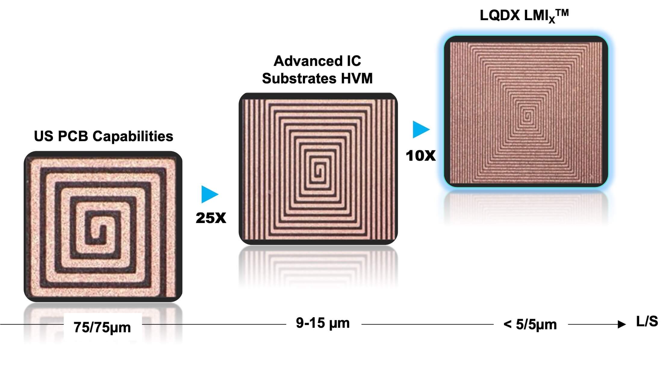
“With Liquid Metal Ink, we can significantly shrink the line/space dimensions beyond what is possible with PVD to increase interconnect density and reduce the number of required layers. This way, we can slow down the trend of larger and more complex substrates to address the warpage issues,” she said (Figure 1).
What the industry needs to develop AI chips is a process that can create very fine structures. Etch processes are used to remove unwanted layers from the surface of the substrate.
But that alone isn’t enough. Beica said getting a thin coating of metal onto the substrate is key. She further explained that the thinner the layer, the faster the etch process will be, which is important for not undercutting the interconnect. Conversely, when the metal layer is too thick, it’s less equipped to support fine interconnects.
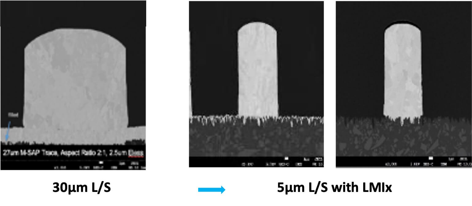
Beica highlighted that other solutions also can’t provide uniform depositions, which means high-aspect-ratio (HAR) through silicon vias (TSVs) can’t be created. TSVs are used for stacking chips vertically by forming interconnects through the wafer or die and are essential for increasing the interconnect density of AI chips. HAR TSVs are interconnects that are much taller than they are wide. Liquid Metal Ink may be one solution (Figure 2)

Beica also shared how LQDX can deposit atomic layer metals straight onto a wide range of substrates, including the Ajinomoto build-up film (ABF), which is the well-known build-up layer used in the most advanced IC substrates, as well as polyimides used for fan-out packaging platforms.
“The industry is looking at different solutions to address the need for ultra-high density interconnects, from adopting adhesion promoters to PVD and even looking at different packaging structures such as 2.xD and organic interposers because scaling beyond 8/8µm L/S into the old good IC substrate is not possible,” she said.
To conclude, Beica shared that Liquid Metal Ink offers both a cost and sustainability advantage over PVD.
“PVD vacuum processing lines occupy four to five times the footprint, with up to 10 times higher installation costs, and five times higher cost/unit,” she said. “LQDX has developed a suite of cutting-edge technologies and processes and can bring a disruptive leap to the industry in interconnect technology.”
Learn more about LQDX and its Liquid Metal Ink technology.


