


At this point, we can’t deny it – we’re truly living in the age of AI. But in today’s changing world where ChatGPT generates information faster than ever imagined, one thing is certain: today’s technology-driven society would not be feasible without advanced packaging.
To help me write this article, I interviewed Damon Tsai and Jiangtao Hu from Onto Innovation to learn about inspection and metrology for AI packages. I gathered a lot from our discussion, but the biggest takeaway was discovering just how high-stress packaging AI chips can be.
First, AI chiplets are complex and expensive because they consist of many “standard” chips stacked together side-by-side and on top of each other using advanced packaging processes. Because of high costs and complexity, the number of working chips on a wafer must be very high. In the semiconductor industry, we refer to the percentage of working chips as yield.
To put this in perspective, a standard 300-millimeter wafer has around 300 chips (interchangeably called die during the pre-packaging phase). So, if 16 of those die are defective, we’d still reach the industry-average yield percentage of 94%. Conversely, an AI chiplet may consist of 50 standard chips. This means one tiny defect will impact >2% yield in an AI chiplet, and the yield percentage already dips below the industry standard. With the high costs (and pressure!) that come with manufacturing AI chiplets, getting a reliable yield is paramount.
With AI chiplets being so valuable, Tsai and Hu mentioned that companies can’t risk losing even a single one. As you can imagine, this is why inspection and metrology are so important.
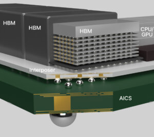
If this doesn’t sound like enough pressure just yet, we’re only scratching the surface. Tsai and Hu shared how companies are increasing the number of stacked chips for added computing power, which makes it even more important to lower the failure rate of each chip. If a high bandwidth memory (HBM) cube increases the stack from 6 to 12 layers, you can see how quickly failure adds up. One defect can ruin the entire stack.
To reduce stack failure, proper inspection during packaging is crucial. When companies stack chips on top of one another, they need to inspect both inside and underneath the chips. This alone introduces a new layer of complexity. In the past, inspection was focused on the surface of the structure. Now, inspectors must make sure there are no bubbles or voids between each chip layer.
Tsai and Hu then explained how Onto Innovation developed a high-speed infra-red (IR) camera to look into each chip by penetrating the silicon. By looking through the silicon, Onto Innovation’s cameras can identify voids between the chip layers at the sub-micron level.
“We have the technology to inspect every chip to make sure the edges, the front, and the insides are okay,” said Tsai. “Inspection slows down the manufacturing process. But customers feel it’s important because the die are so expensive. Throughput is important, but yield is more important.”

“Throughput” refers to the time it takes for a chip to complete the manufacturing process. More chips processed in less time means a company may have more chips to sell, but it does not mean the chips are necessarily working. The percentage of working vs. defective chips is what’s referred to as yield. Companies are always trying to balance high throughput with high yield.
Lastly, Hu shared that inspection and metrology of AI packages is an ongoing process.
“In the past, inspection and metrology have been separate steps,” said Hu. “In the era of AI chiplets, there’s more demand to inspect and measure every die at every step, and we see a growing trend of metro-inspection for advanced packaging processes.”
Learn more about Onto Innovation’s inspection and metrology processes.


