


The Boston Consultant Group (BCG) recently took a look at the impact that advanced packaging is having on the microelectronics chip ecosystem. Let’s take a look at some of the points that they make.
Advanced packaging is replacing simple “scaling”, which had been the traditional way to achieve advancements in the past. An advanced multichip package incorporates multiple chips and processes into one component. This approach directly addresses the most critical semiconductor technical and commercial constraints. (Figure 1)
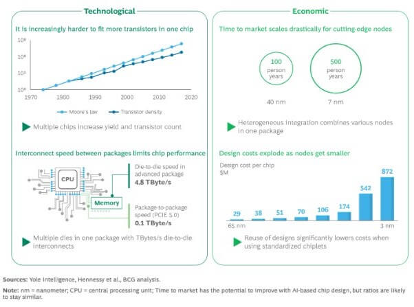
Advanced multichip packaging improves performance and time-to-market while reducing chip manufacturing costs and power consumption.
IFTLE would be remiss not to point out that this has been the concept since the 1990s when these multichip packages (MCPs) were called multichip modules (MCMs). Indeed through the late 1990s and early 2000s the IMAPS MCM Conference, held yearly in Denver, drew 500 – 1000 attendees yearly to focus on nothing but this concept. The point being the drivers for multichip packaging have been around for 30+ years. This in itself is not new. What is new is the fact that this has now become one of the primary methods of advancing microelectronic performance.
BCG further points out that “…for chipmakers, investors, and computing device and equipment makers, the emergence of advanced packaging represents a radical shift in the semiconductor industry landscape. The next generation of industry-leading organizations will be those that realize value creation is migrating towards companies that can design and integrate complex, system-level chip solutions using concepts like advanced packaging. Merely making individual components will rapidly lose luster, replaced by collaborative efforts that bring together the best in design, packaging, and system integration to meet the demands of the market.” Certainly, all readers of IFTLE would agree.
BCG uses 4 excellent examples to illustrate the advantages of advanced packaging (Figure 2).
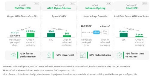
According to BCG, the NVIDIA H200 is an AI-core GPU. Six HBM memory stacks are packaged with the central IC chips, resulting in interconnection speeds of up to 4.8 TB/s. Conventional systems, where chips are connected via a printed circuit board, are typically limited to less than 200 GB/s. Close interconnect distances also drastically decrease the power consumption of these chips, making the data more economically feasible.
In the AMD Ryzen series, using chiplets rather than a single large system-on-chip (SoC), cut manufacturing costs by as much as 50%. The smaller die sizes contribute to this cost reduction by increasing fabrication yield rates because the same number of defects on a wafer is distributed across more dies.
By integrating the chips used in Optireg linear voltage controllers into a single package, Infineon claims it was able to reduce the part’s footprint by 60%. Optimizing for smaller size has high impact in applications such as mobile devices, small medical equipment like hearing aids and pacemakers, and automotive computing systems.
Intel claims it has already shown that switching from a single large SoC to multiple dies in its Data Center GPU Max Series can minimize die complexity and allow existing die designs to be reused in multiple packages. In the process, Intel says it can reduce time to market by up to 75%.
BCG points out that while consumer electronics like smartphones currently dominate advanced packaging applications, AI will likely propel future growth. AI requires rapid data exchange between computing and memory elements, which is enabled by 2.5D and 3D packaging. These approaches place more than two chips next to each other to generate high interconnect speeds at a relatively low cost. AI applications account for 25% of the total advanced packaging market already, and this is poised to grow at around 20% per year through the next decade.
Traditionally, the value chain of chipmaking was rather simple: one chip designer, one front-end manufacturer, and a back-end company for packaging and testing. Sometimes all these roles were handled by the same IDM. In this scenario, the lion’s share of value capture is concentrated in chip design and the front end—where most of the innovation lies—while packaging is relegated to a lower-margin role (Figure 3).
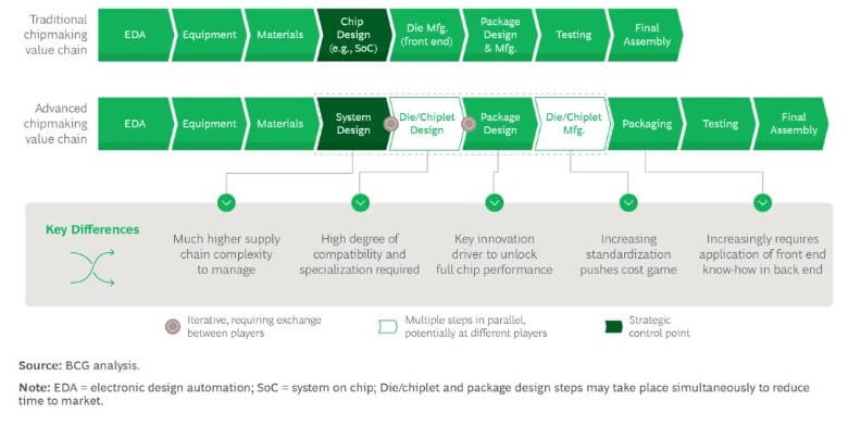
But as the package becomes a core determinant of system performance, multiple semiconductor dies—often designed and manufactured by different companies—will have to be integrated in the same package. System designers will need to control this more complex supply chain and drive close collaboration and alignment among all players.
BCG contends that the primary changes in chip ecosystem will be evident in:
1) Elevating the Role of System Design
The value share contributed by advanced package design will rise significantly, underscoring its strategic importance. Chip designers are extending design from the single chip to the whole system, including integrating multiple dies into an advanced package.
2) Shifting from Front End to Back End
The package will become a point of innovation, a differentiation driver pivotal to system performance. While front-end manufacturing will continue to command a high share of value generation, back-end design and packaging will gain in importance and profit value.
3) Adapting to Complexity
Electronic design automation (EDA) software must be programmed to design and simulate multiple chips in a package and how their interplay may impact operating conditions, such as thermal dissipation and warpage. Similarly, materials suppliers must develop new, innovative materials to address, among other things, thermal expansion and heat transfer at the numerous interfaces in advanced packages. And packaging equipment must be modified to meet the decreasing feature sizes and increasing precision requirements of advanced packaging.
The Altered Face of the Chip Ecosystem
These technology changes will alter the semiconductor industry in significant ways. There will be a much greater degree of collaboration across chip design, package engineering, and system architecture, as each will directly impact the other.
Proposed Strategic Solutions for Semiconductor Players
Fabless Chipmakers
Fabless chipmakers, who design chips and partner with foundries for manufacturing, will have to expand their business models as the single chip becomes part of an advanced multichip package. This comes with the challenge of managing a complex supply chain across other chip designers, multiple foundries, and even material suppliers.
Foundries
BCG says it sees advanced packaging threatening the revenues of leading-node foundries as it reduces demand for large monolithic SoCs, replacing them with smaller, more standardized dies. To maintain their profit levels, leading-node foundries should extend their offering into advanced packaging, positioning themselves as system foundries. IFTLE adds that obviously this is already happening with TSMC, Samsung, Intel now being the leaders in advanced packaging solutions.
BCG sees foundries focused on mature nodes struggling to develop advanced packaging solutions that can compete with those of their leading-node peers. IFTLE adds again that we have already seen this occur.
Integrated Device Manufacturers (IDMs)
Traditionally, IDMs design, manufacture, and package their own chips, even if parts of the value chain may be outsourced. BCG sees the economics of this business model may be challenged in an advanced packaging environment where system designers increasingly demand unpackaged dies for integration into other suppliers’ packages, limiting demand for the IDMs packaged end product. Leading IDMs may be able to capture the system designer role themselves, particularly for lucrative, specialized applications.
Outsourced Semiconductor Assembly and Test (OSATs)
“In the new packaging world, OSATs need to determine their most advantageous position between simple wire bonds and the most advanced 2.5D/3D packages.” BCG further suggests that OSATs should build on their traditional strengths focusing on essential packaging activities that will still be required for some time, such as bumping.
BCG concludes that “In the dawn of the advanced packaging era, ….. companies that recognize and invest in the strategic value of advanced packaging are setting themselves up for success. …..
“…for investors, strategic partners, and semiconductor companies, the message is clear: the time to invest in and prioritize advanced packaging is now. Those that do will thrive, steering the semiconductor industry towards its next performance frontier and into a future marked by ingenuity, speed, and sustained growth”.
For all the latest in Advanced Packaging stay linked to IFTLE……………………………


