Executive Summary: Innovative, High Throughput Surface Metrology
Hybrid bonding is enabling the next generation of advanced packaging in the semiconductor industry. As hybrid bonding occurs at the molecular level, it requires careful control of the surface topography for high yield.
At Adeia, we developed new methods to improve both throughput and assembly yield in the overall assembly process. The first concept we developed is an optical interferometry-based surface metrology technique that measures Cu interconnect recess over 1000x faster than the standard AFM technique. The second is an implementation of a convolutional neural network (CNN) for automated defect inspection. The CNN was trained for the most relevant defects attributed to hybrid bonding yield loss.
Both innovations increase the throughput of sample screening without sacrificing data fidelity or reliability. The increased throughput enables faster product development with enhanced yield, thereby improving cost and time to market.
Key Factors for Surface Metrology for Hybrid Bonding
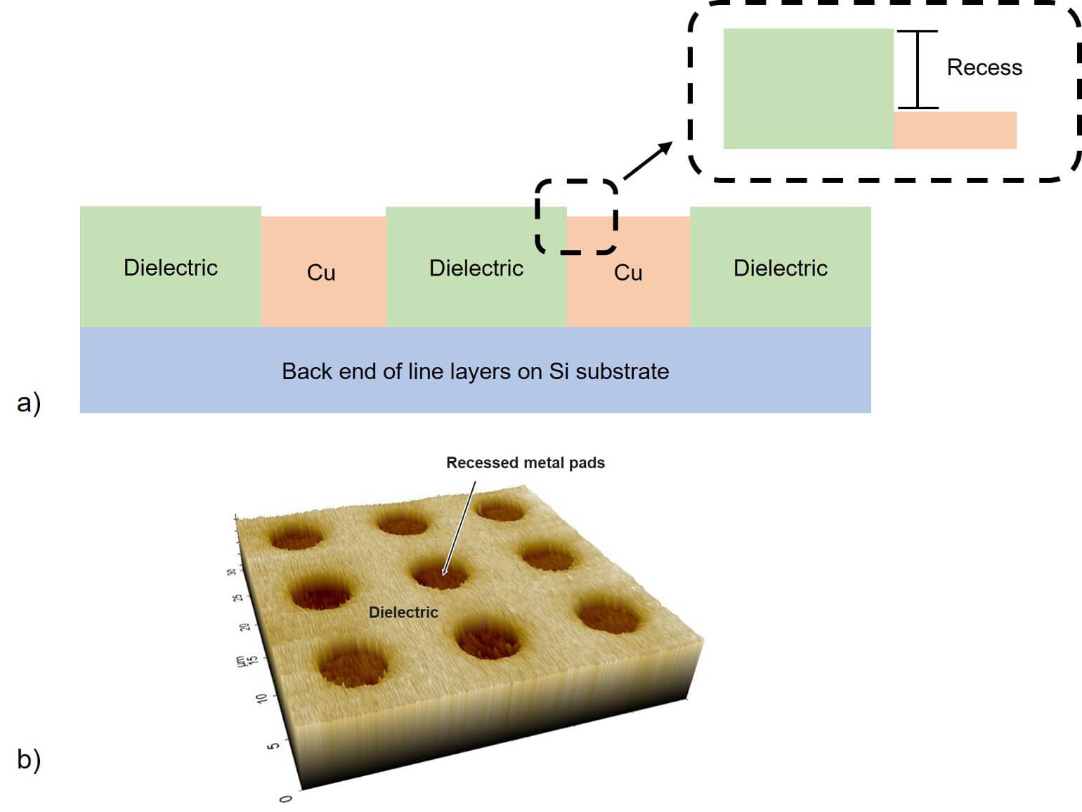
Two important parameters for die and wafer inspection are metal recess and defectivity. Recess is defined as the depth of the metal interconnects, typically copper, with respect to the dielectric surface (Figure 1).

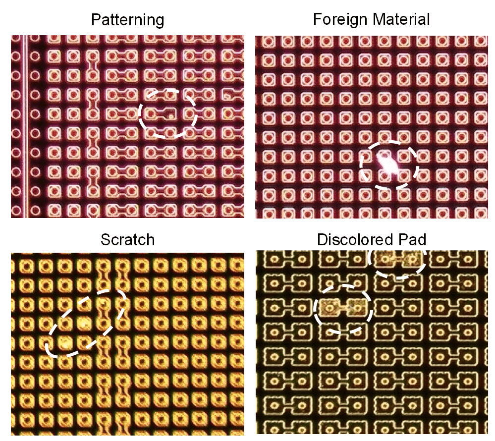
The Cu recess may be controlled through careful chemical-mechanical polishing (CMP) within the damascene process. Defectivity is a measure of the surface flaws in the material. Defect examples include foreign material due to particles in the air, metal corrosion, lithography pattern defects, and scratches from the CMP step (Figure 2).

The surface characterization accuracy is critical when driving toward high-throughput characterization. High-throughput data collection enables larger datasets, leading to improved understanding of process-materials and parameter-performance relationships. Accurate characterization at higher throughput leads to shorter manufacturing cycles.
Statistical Study of Copper Recess with 1000x Higher Throughput
Atomic force microscopy (AFM) is the standard method to measure Cu recess. AFM is a surface characterization technique where a probe tip at the end of a cantilever is scanned over the surface of a sample. The topography of the sample is measured based on the deflection of the cantilever from the probe tip interaction with atomic forces on the surface of the sample.
AFM is widely accepted because the data is extremely reliable, and it offers nanometer-scale resolution in X and Y and ~ 1 Angstrom resolution in Z. However, probe-based AFM is slow. Imaging an 80µm by 80µm area takes ~5 minutes, forcing lower sampling statistics per wafer.
Optical interferometry, a non-contact technique, records surface topography data with high throughput. It uses the interference of reflected light from a sample surface with a reference light beam to measure the height of surface features.
The throughput of optical interferometry is about 1,000 times faster than AFM with a resolution of 0.5 µm in X and Y, and a few nanometers in Z, and is dependent on material composition. If the surface is composed of different materials, e.g., Cu from the pad surface and SiO2 from the dielectric surface, the apparent topography is different from the actual due to the different material optical responses.
In our 2024 ECTC paper entitled, “High-Throughput Characterization of Nanoscale Topography for Hybrid Bonding by Optical Interferometry,” we present a method to calibrate the interferometry for a Cu/SiO2 hybrid bonding surface and study its topography with greater than 1,000 times higher throughput.
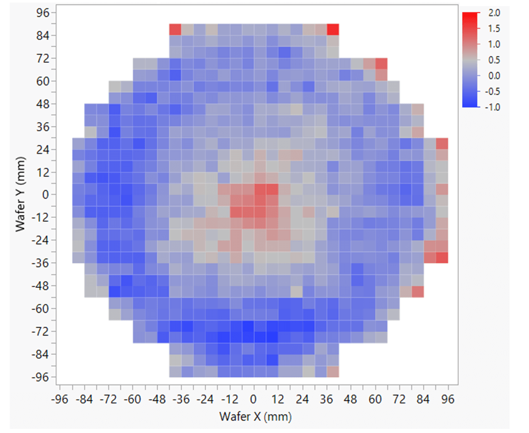
With this method, we can obtain larger quantities of reliable data, revealing new insights into the statistical distribution of Cu recess across a wafer. Maps of metal recesses across a wafer can be created in a reasonable time frame (Figure 3), and CMP process conditions used to control recess can be tuned with more confidence during process development.

Our 2023 ECTC paper [1] briefly described the idea, and the 2024 paper will present the full details of the technique using multiple examples.
Measuring Defectivity with Convolutional Neural Networks
Optical imaging is the standard method of identifying defects on the surface of samples due to its speed and accuracy. Depending on the pad and pitch size, inspection systems take hundreds to thousands of images across a single wafer to determine defectivity on the wafer. The task of image defect identification and recognition is perfect for the CNN model application. CNNs are regularly used in image recognition problems to identify features and categorize defects.
At Adeia, we implemented CNN models and trained them with our own dataset of a few thousand images of wafer and die surfaces, which were collected with dark field imaging on an automated microscope stage.
Our CNN model identified defects at a higher rate than a highly trained human operator and flagged defects that are known to negatively affect yield in hybrid bonding samples. Details of the CNN architecture, the training data, and the effectiveness of the models will be explained in detail in our 2024 ECTC paper, “Deep Convolution Neural Networks for Automatic Detection of Defects which Impact Hybrid Bonding Yield.”


 Dr. Bongsub Lee is the Director of Design and Analysis at Adeia in San Jose, California. He is working on hybrid bonding technology, especially regarding materials characterization, device design, and supply chain management. He received his PhD in Materials Science and Engineering from the University of Illinois at Urbana-Champaign and his master’s and bachelor’s degrees from Seoul National University. He made more than 60 publications, which have been cited more than 2700 times in total.


