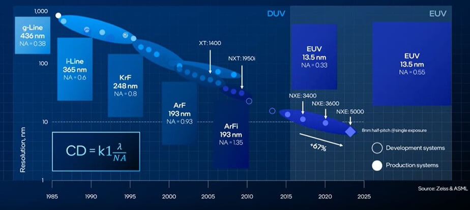
In 1987, the lithography team I worked with returned from SPIE and presented our findings from the conference. Ultra-violet (UV) lithography was just crossing the 1µm line widths, and the industry was looking for what might be next to replace it.
At that time, e-beam lithography was still in contention for production lithography, but it had not had much success in chip patterning in the facility where I worked. X-ray lithography was mentioned as a possibility for the future, and of course, deep ultra-violet (DUV) lasers were also emerging at that time.
Fast forward to my days as an analyst in the early 2000 and invitations from Lawrence Livermore National Labs (LLL) started to cross my desk on extreme ultra-violet (EUV) lithography. A considerable EUV consortium from the industry was working on the topic at LLL. They discussed progress at an annual open house. ASML was heavily involved at this time, as they had acquired SVG group, which was due to the US EUV technology development before 2000.

Fast forward to 2024 and ASML and Intel are firing up the latest advances in lithography. The 0.55NA TWINSCAN EXE:5000 system has been shipped, installed, and is getting ready for first light at the Hillsborough Oregon facility. Meanwhile, ASML has achieved patterning 10nm features at IMEC in preparation for process transfer to Oregon.
Intel was an early investor and participant in developing EUV technology but opted to stick with 193i multiple patterning. Some, including Pat Gelsinger, suggest this is one of the reasons Intel fell behind in the chip technology race. To catch up and achieve Intel’s technology roadmap, the high NA systems will be introduced at Intel’s 14A technology nodes.
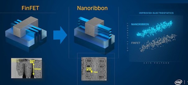
The 14A node coincides with two important technology features: Intel’s second-generation ribbon FETS or GAA technology, and the second generation of power via. While the power via, which is sometimes referred to as backside power, will use DUV lithography, the 14A ribbon FET will take advantage of the high NA technology, and enable the transistors to use one mask layer and not multiple patterning to print the features.
Implementing ribbon FET – also called gate all around (GAA) – is important to achieve better performance in the transistor and as the industry looks towards CFETS in the future. In CFETS the ribbon FET will be stacked on top of each other using monolithic 3D processes. This technology insertion is estimated to arrive in the 2030 time frame, possibly soon after 14A reaches high-volume production. The High NA system will be a major enabler at this process node as the monolithic transistor stacking begins to take place and moves the transistor further into the 3D realm.

While it doesn’t need high NA EUV for processing, the power via has significant benefits for logic processing. It significantly reduces process complexity in the back-end-of-line (BEOL) and improves chip power consumption.

According to IMEC, backside power can also benefit the industry as it continues to move to 3D packaging, as it enables improved connectivity to other die and substrates while reducing power consumption. Reducing power consumption in the chip and packaged system is critical for the future, especially in AI where large language models are consuming enormous amounts of power. With the concern about power consumption for AI and blockchain applications, reduction at the chip level will be an important part of chip sustainability in the future.
As Intel and the rest of the industry move forward on technology nodes and 3D packaging it will employ a wide bandwidth of advanced lithography tools. 248nm, i line, and nanoimprint lithography will see significant use in the advanced packaging space. Intel has also introduced Direct Self Assembly with the high NA process to help with pattern definition. While the bulk of the lithography industry revenue will go to EUV and 193i equipment, 248 and i-line will not be going anywhere soon and will play a significant role in 3D packaging well into the future.


