


Hybrid bonding enables an assortment of possible chip architectures, mainly targeted at high-end applications including high-performance computing (HPC), artificial intelligence (AI), servers, and data centers. As the technology matures, further growth is projected into consumer applications, memory devices including high bandwidth memory (HBM), and mobile and automotive applications that could benefit from high-performance die-to-die connections.
The Back Story on Heterogeneous Integration
Part of the fun of playing with building blocks is the seemingly unlimited ways that one can put them together. Imagine adopting this concept to the semiconductor industry where you can take different kinds of chips and combine them like blocks to build something unique. Start with defined goals for performance, size, power consumption, and cost for your semiconductor product, then aim to meet the requirements by combining different types of chips into a single package. This concept of the heterogeneous integration of chips is already driving innovation across packaging technologies (Figure 1).
The adoption of heterogeneous integration in packaging has been accelerating recently to meet the increasing need for more complex functionality and lower power consumption. Heterogeneous integration allows IC manufacturers to stack and integrate more silicon devices in a single package. This can include the combining of chips from different wafers, from different semiconductor technologies, and from different suppliers. Heterogeneous integration also enables chiplet integration to overcome yield challenges for large die, as well as reticle size limitations.
As 2.5D, 3D, and fan-out packaging technologies have evolved, copper microbumps have provided the required vertical metal device-to-device interconnections into a single, integrated product. Copper microbumps, typically 40µm in pitch (25µm bump size, 15µm spacing), have scaled down to 20µm and 10µm pitch to increase package density and functionality. Below 10µm bonding pitch, however, microbumps begin to run into yield and reliability challenges. So, while traditional copper microbumps will continue to be used, new technologies are also being developed to continue increasing interconnect density. Hybrid bonding technology is emerging as a viable pathway for high-end heterogeneous integration applications where the interconnect pitch is 10µm and below.
What is Hybrid Bonding?
Hybrid bonding is a process to create a permanent bond between heterogeneous or homogeneous die. “Hybrid” refers to the fact that both dielectric-to-dielectric and metal-to-metal bonds are formed between the two surfaces. The use of tiny copper pads embedded closely together in dielectric delivers up to 1,000X more I/O connections than is possible with copper microbumps and is driving signal delay to near zero levels. Further advantages include expanded bandwidth, higher memory density, and increased power and speed efficiencies.
Hybrid Bonding Technologies
The key process steps include the preparation and creation of the pre-bonding layers, the bonding process itself, the post-bond anneal, and the associated inspection and metrology at each of the steps to ensure a successful bond.
There are two ways in which hybrid bonding can be accomplished: wafer-to-wafer (W2W) and die-to-wafer (D2W) (Figure 2).
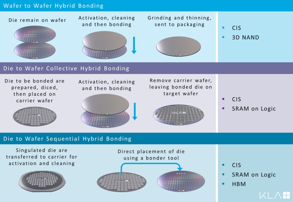
D2W is the predominant choice for hybrid bonding in heterogeneous integration as it supports different die sizes, different wafer types, and known good die, all of which are generally not possible for W2W schemes. For each, the wafers are first manufactured in a semiconductor fab before a hybrid bonding process is utilized to stack the chips vertically.
Hybrid Bonding Shifts Packaging Toward the “Front End”
Hybrid bonding takes place in an environment that must satisfy requirements for contamination control, factory automation, and process expertise due to the advanced process requirements and complexity involved – not in a typical packaging house like many other packaging integration methods. To prepare the wafers for bonding, additional front-end semiconductor manufacturing processes are utilized to create the final layers on the wafers to connect the chips. This includes dielectric deposition, patterning, etching, copper deposition, and copper CMP. The semiconductor fab has the requisite environmental cleanliness, process tooling, process control systems, and engineering expertise for the hybrid bonding processes.
Known Good Die are Required
Using D2W hybrid bonding to achieve the heterogeneous integration of multiple die into one package results in a high-performance, high-value device. The stakes are high when you consider that including one bad die could cause the entire package to be scrapped down the line. Using only known good die is required for maintaining high yields. Optimization of the process and the implementation of sensitive process control steps are required for achieving die integrity to increase the number of viable die, as well as providing accurate information required to sort good die from bad before entering a process like D2W bonding.
Void-free Bonding for High Yields
Void-free bonding depends upon the successful bonding of both the dielectric areas and copper pads. During the bonding process, the initial bond occurs at the dielectric-to-dielectric interface at room temperature under atmospheric conditions. Subsequently, the copper metal-to-metal connection is formed via annealing and metal diffusion.
The hybrid bonding surfaces must be ultra-clean, as even the tiniest of particles or thinnest of residues could disrupt the process flow and cause device failures. High-sensitivity inspection to find all defects is required to verify that the die surface remains clean for successful void-free bonding.
SiCN has been shown to offer a higher bond strength than alternative dielectrics such as SiN or SiO2. Recent development work[1] has demonstrated plasma-enhanced chemical deposition (PECVD) of SiCN at a temperature low enough to satisfy the limitations of any temporary bonding layer (<200°C). The properties of the film also include the required stability to avoid desorbing hydrogen or hydrocarbons (which can result in void formation) as the temperature is increased for the subsequent copper annealing (>350°C), once the temporary bonding layer has been removed.
Before hybrid bonding, the copper pads must have an optimal, dished profile to allow the copper to expand during the metal bonding process (Figure 3).
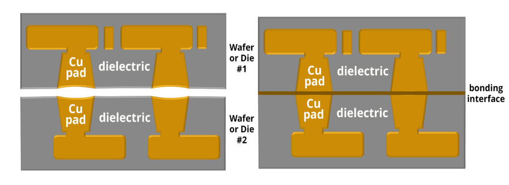
A shallow and uniform copper recess is necessary to achieve void-free bonding. Here, high-resolution metrology can be used to monitor and drive process control and improvements.
![[err-ad-fallback-title]](http://www.3dincites.com/wp-content/plugins/a3-lazy-load/assets/images/lazy_placeholder.gif)
Plasma Dicing for Cleaner, Stronger Die
Many potential sources of voids, defects, and non-uniformities must be carefully controlled at each process step. Even a particle as small as 100nm can result in hundreds of failed connections and a defective stacked package. For example, in the case of D2W hybrid bonding where individual die are diced before being transferred and bonded to a second whole wafer, traditional methods of dicing such as a mechanical saw or laser grooving/dicing can introduce particles or surface imperfections, particularly at the die edges[2], which can interfere with the subsequent hybrid bonding process. Plasma dicing is an alternative method that has already been proven in high-volume production, in specific applications, where the benefits such as more die per wafer or increased die strength outweigh any increased processing costs. In the case of hybrid bonding, the plasma dicing process results in an extremely clean die surface and edge with no particulate contamination or edge chips associated with blade dicing, and no laser debris/recast/laser groove cracks. Plasma dicing die before hybrid bonding will result in more consistent bonding with lower defectivity and higher device yields.
Hybrid Bonding Process Control
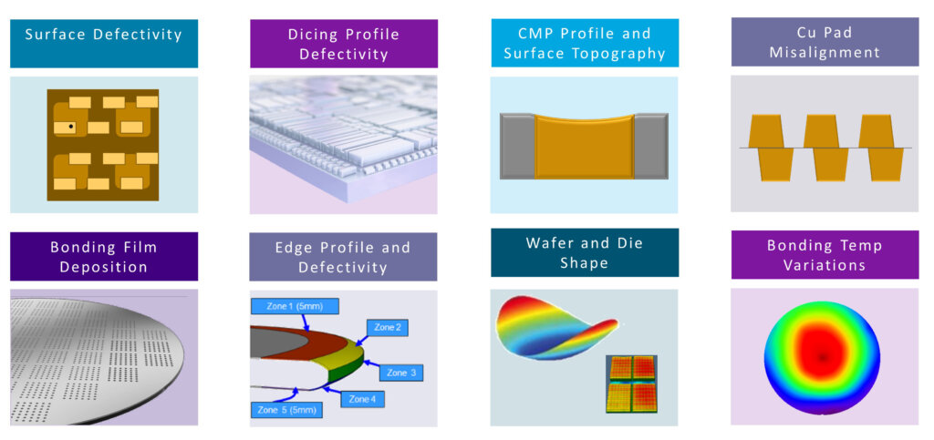
To enable hybrid bonding to successfully transition to high volume manufacturing (HVM) with high yield, process control is critical. Pre-bonding non-uniformities across the wafer, voids, and other defects can directly interfere with the copper interconnects during the bonding process and degrade product yield. Additional sources of non-uniformities that impact the bond include CMP profile and surface topography, copper pad misalignment, wafer shape, and variations in bonding temperature. Each of these issues must be carefully measured and controlled at the source (Figure 4).
Some key process control requirements for hybrid bonding include:
- Film Thickness and Uniformity: Dielectric film thickness to create the final pre-bonding layers must be carefully controlled, within a die, across the wafer, and wafer to wafer.
- Overlay Alignment: To successfully bond surfaces with a very small pitch (currently ~1-10µm), tight control of the bond pad alignment is required to make sure the copper pads to be bonded line up perfectly, driving an increased need for overlay metrology precision and die-bonder control.
- Defectivity: The direct dielectric-to-dielectric and copper-to-copper bonds in hybrid bonding require a much cleaner surface free of particles and residues to minimize voiding at the interface. This drives the adoption of optimized processes like plasma dicing along with significantly higher inspection sensitivity and stringent defect reduction efforts compared to conventional solder-bump interfaces.
- Profile and Roughness: Successful bonding requires surface profile and roughness controlled to the nanometer level, requiring significantly more precise metrology to help develop and control the preparation of the pre-bonding surface in an HVM environment. Before bonding, the copper pads must have a specific dished profile.
- Shape and Bow: Both W2W and D2W hybrid bonding can be sensitive to wafer shape and bow, requiring an increased need for wafer-level and die-level shape metrology for characterization and control.
There are additional process and process control steps required after the actual bonding process, such as inter-die gap fill in D2W bonding where the dielectric is deposited in between, and over the top of the separate bonded die. With appropriate stress control measures, PECVD can produce extremely thick (~30-40µm), crack-free SiO with a TEOS precursor, which is capable of withstanding subsequent steps, such as CMP and lithography.
The scaling to smaller feature sizes and complex 3D integration schemes shifts packaging processes from packaging houses to front-end semiconductor fabs. KLA’s wide range of advanced process control and crucial process solutions uniquely help to enable and advance hybrid bonding adoption.
References
[1] S Iacovo, et al “Direct Bonding Using Low-Temperature SiCN Dielectrics “2022 IEEE 72nd Electronic Components and Technology Conference (ECTC), p602-607
[2] F Inuoe et al “Advanced Dicing Technologies for Combination of Wafer to Wafer and Collective Die to Wafer Direct Bonding” Proc 2019 IEEE 69th Electronic Components and Technology Conference (ECTC), p437-445
This article first appeared in the 2023 Yearbook. Read the issue here.


