After two years of virtual conferences, it was great to be back in person last week at the 2022 IMAPS Device Packaging Conference (IMAPS DPC). With over 400 attendees, it felt like the good old days. While it wasn’t the first in-person conference we’d attended; it did feel more like things were getting back to normal. Spirits were high, handshakes were ok, masks were optional.
For IMAPS and 3D InCites, it was the perfect launching ground for our new official industry partnership. You’re going to see a lot more collaborative projects brewing between the two organizations.
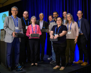
At IMAPS DPC, we held the 3D inCites Awards Ceremony just after the Tuesday morning keynotes (Figure 1). As the official podcast of IMAPS DPC, we set up a recording “studio” in our booth in the exhibit hall and had a steady stream of live interviews with keynote speakers and IMAPS dignitaries, as well as 3D InCites award winners and community members. We’ll be dropping those episodes over the next few weeks.
 By Wednesday evening, attendees were ready to relax and enjoy our first annual DEI Fund Night. The 2022 Mural project (Figure 1) provided a great backdrop for our annual photo booth. Party-goers enjoyed some cornhole competition, and Tim Olson’s team at Deca brought their Space Invaders game to the party. All donations from the game went to the DEI Fund. Thanks to this year’s donors: ASE Group, EV Group, KLA, Evatec, YES, CyberOptics, Veeco, Kiterocket, ERS electronic GmbH, Micross, Amkor Technology, Deca, Cadence, 3D Plus, Gel-Pak, Mosaic Microsystems, StratEdge, and Namics.

Finally, on Thursday afternoon, while some hit the links in support of the IMAPS Foundation, a bunch of us non-golfers hit the hiking trails for the first Annual Hike For DEI, sponsored by KLA, with hydration provided by Amkor Technology. While we are still tallying up the final donations, it’s safe to say that we’ll exceed last year’s $20K seed donation to the 3D InCites’ DEI Fund.
Topics of Conversation at IMAPS DPC
In 2018, fan-out was all the rage. The conversation has shifted since then, and so has Bora Baloglu’s license plate. (not to mention his car) (Feature Photo). This year, we heard a lot about chiplets, hybrid bonding, and onshoring in the keynote talks at this years’ IMAPS DPC and co-located Global Business Council.
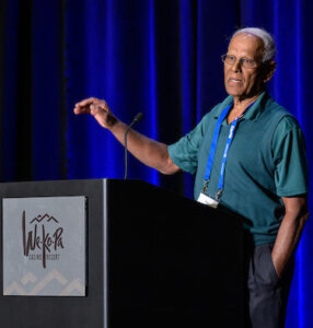
Rao Tummala, of Georgia Tech, (right) came out of retirement to deliver the opening keynote about future packaging (not to be confused with “the future of packaging.”)He reminded us that it takes (at least) 10 years for new technology to go from concept to manufacturing. In some cases, it takes much longer, until there is an application that needs that concept.
Tummala claimed to have invented the chiplet packaging concept in the 1980s while at IBM. But he called it system-on-package (SoP), not chiplets. I first heard Tummala talk about this concept for system scaling in 2006. Don’t confuse SoP with today’s System IN package (SiP), which integrates disparate technologies into a single package. But as with most things advanced packaging, it took decades for the SoP concept to evolve into what we refer to as chiplets today. More on that later.
The purpose of packaging has also changed over the years, explained Tummala. It used to be all about interconnection, power, thermal, and protection. In this new “Packaging Era”, packaging becomes a strategic value-add. It can improve performance, cost, and system reliability.
“We used to get 30-40% improvement from node to node. Today we don’t get that,” he explained. “With finer and finer lines, we have interconnect delays. We need to bring ICs closer together. Lots of wires don’t solve the problem. It must be designed in.”
He also is betting on optoelectronics taking off, as it offers better bandwidth and power efficiency. He says it hasn’t happened until now because as with everything companies don’t change until there is no other way.
At Georgia Tech, glass packaging is all the rage. They’ve been working on it for years and have recently demonstrated 1µm RDL line/space. One application is to use a glass interposer between the logic and memory stack so that through-silicon vias (TSVs) aren’t needed in the logic die. I’ll be curious to see if this makes it to manufacturing in the next ten years.
3D Chiplets Are Here
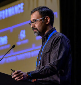
In his keynote, AMD’s Raja Swaminathan(left) explained that high-performance computing applications need 2X more compute power every 1.2 years – much faster than Moore’s Law. He said the slowing of Moore’s Law combined with the increasing cost is causing technology headwinds to meet these demands. AMD has set an efficiency goal for HPC and artificial intelligence (AI) applications. Through architectural innovations, package, and silicon technology advances, the company plans to accelerate the energy efficiency rate by 30X by 2025.
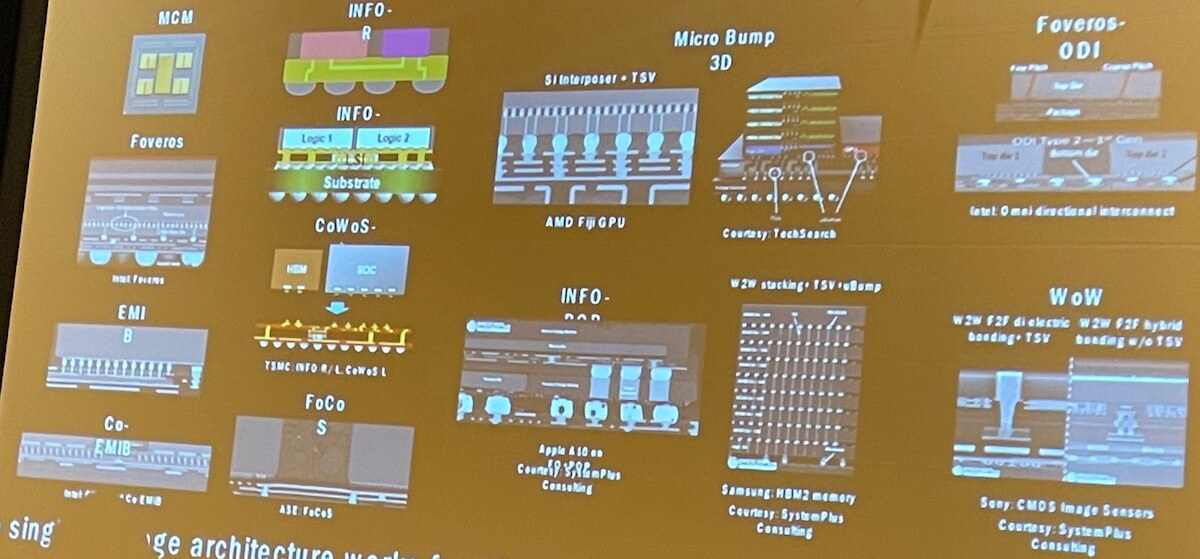
Chiplet integration is the key, notes Swaminathan, because it enables a more flexible approach. He says this is not a one size fits all approach, and it depends on the end products. There are multiple packaging architectures for chiplets and the choice depends on power, performance, area, and cost (PPAC) (Figure 2).
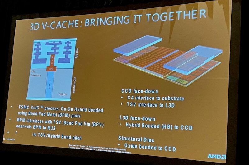
Swaminathan then described AMD’s latest chiplet design; the one that won them the 3D InCites Device Technology of the Year award (Figure 5). It is the industry’s first high-performance processor product built using hybrid bonded 3D cache die. It implements both hybrid bonding and through-silicon vias (TSVs). It improves effective memory latency, reduces long data path and I/Os dynamic powers, and fits more transistors within a given package cavity size.
The Final Word: SiP or Chiplets?
Because I knew someone was going to say that chiplets are just a new name for multi-chip modules (MCMs) or system in package (SiP), I decided to take the bull by the horns bring up the topic myself. I asked Swaminathan: What makes chiplets architectures different than your garden variety system-in-package (SiP)? I already knew the answer, because I’ve been asking this question of everyone I speak to, but I wanted the audience to hear it for themselves.
Here’s the key differentiator: SiPs comprise chips that can function independently of each other. They can stand alone as single packaged chips. In a SiP configuration, they are integrated with disparate technologies to create a complete system in a smaller footprint. Chiplets, however, are designed to work together. A single chiplet can’t be packaged as a unit and function on its own as a single die. It must be integrated with other chiplets to function properly.
Hybrid Bonding Update
Speaking of hybrid bonding – and there’s hardly a presentation that DOESN’T mention it – Xperi’s Laura Mirkarimi provided an update on the company’s proprietary DBI Ultra – die-to-wafer (D2W) hybrid bonding approach. Chiplet architectures, such as AMD’s V-Cache, stand to benefit greatly from this highly parallel interconnect process.
In a nutshell, DBI Ultra is scalable to below 1µm. “If you can print it, we can bond it,” says Mirkarimi. It’s flexible and can be performed with different dielectrics and metals. The only caveat is that it requires a tool that can achieve high-accuracy placement.
Mirkarimi explained that this D2W hybrid bonding delivers enhanced electrical and thermal performance over Cu thermocompression bonding. It also makes die stacks perform as well as a single die. It requires 11 fewer wafer process module steps over solder bumps; five from the front end and six from the back.
Recent reliability shows that thermal performance is better because there is no heat conductivity through the layer. The Cu-cu bond provides both hermeticity and dielectric protection in the device. And in a fine pitch test vehicle to measure coarse vs. fine pitch interconnect, even with 80% shift off the pads, electrical performance was still excellent.
The innovation going forward involves finding new application spaces and investigating if very large die can also be bonded void-free.
3D InCites Podcast: Are You Listening?
We captured some of the best conversations of the week in our podcast interviews. For example, we talked about onshoring advanced packaging with Darrin Crum, who heads up the DoD’s state-of-the-art heterogeneous integration and packaging (SHIP) Program, Tom Smelker, VP/GM Microsystems at Mercury Systems; John Lannon of Micross AIT; and Jim Will of Skywater. We also had a conversation with IMAPS president, Beth Keser, and President-elect, Erica Folk, who talked about their vision for the future of IMAPs to make it better than ever. Lastly, we interviewed our award winners and some of our community members. We’ll be dropping those episodes over the next few weeks. You can find them here or follow along wherever you get your podcasts. ~ FvT


