


Electronics Packaging vs. Advanced Packaging
Electronics packaging is generally divided into three major areas, traditional packaging – also called standard or mainstream packaging, and sometimes even just “Others”: advanced packaging and emerging packaging technologies.
Traditional packaging is everything with wire or ribbon bond interconnects on a ceramic, metal lead frame, or organic laminated substrates, and it is typically a single die package. Advanced packaging starts with flip-chip interconnects (bumps, micro-bumps, Cu-pillars), mainly on organic laminated substrates, and has been transitioning during the last decade into wafer-level packaging (WLP). This includes:
- Fan-in packaging with thin-film processed redistribution layers (RDLs)
- fan-out packaging at the wafer and panel level (FOWLP, FOPLP) using either chip first – RDL last, or RDL first – chip last, face-up and face-down approaches
- So-called 2.5D interposer technology with through-silicon vias (TSV) with passive – or more recently active interposers
- 3D packaging such as die stacking, package stacking with through package vias (TPV), which can be pre-formed or post-formed, e.g.
- Thru mold via (TMV)
- Through glass via (TGV);
- 3DIC with TSV via first, via middle, and via last concepts
- System-in-package (SiP)
- And many different combinations of the above, which are summarized under the term Heterogeneous Integration (Figure 1).
Heterogeneous Integration Roadmap
Under the title Heterogeneous Integration Roadmap (HIR): Driving Force and Enabling Technology for Systems of the Future, the executive summary of the roadmap talks about the vision of the HIR, which is available to everyone.
“It became one of the most important roadmaps in the semiconductor world, after the International Technology Roadmap for Semiconductors (ITRS) was discontinued. The SIA7 (Semiconductor Industry Association) brought the ITRS to closure in July 2016, but we are now in a new world order with changes and disruptions that we could never have imagined before. The executive summary continues… “the need for roadmapping has never been clearer. The business landscape is experiencing great change with the continued rise of technology companies that are driving social media, cloud computing, search, online commerce, and big data, leading to integrated hardware-software driven applications and unprecedented growth of application spaces”.
Electronics Packaging Market
Looking at the electronics packaging market, we are seeing fast growth and new opportunities. The opportunities are not only for the typical players in this market: the outsourced semiconductor assembly and test service providers (OSATs), integrated device manufacturers (IDMs) and electronic manufacturing service (EMS) companies, but also for foundries and material suppliers stepping up in the value chain and taking over an increasing share of the advanced packaging market.
According to Yole Développement in France, the total packaging market is predicted to grow from $53.2B in 2014 to $85B in 2025. Advanced packaging is going to count for 49% of that, coming from 38% in 2014. That is just an 11% higher share, but as the total packaging market is growing, the revenue in advanced packaging is predicted to more than double from $20.2B in 2014 to $42B in 2025. In 2019, wireless communication and consumer applications generated 85% of advanced packaging revenue (Figure 2).
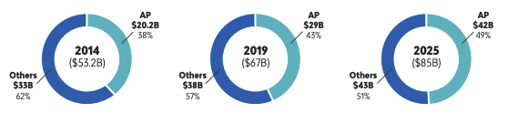
Also, the traditional packaging market revenues are going up by more than $10B from $33B in 2014 to $43B in 2025. It is just its share in the total packaging market, which is growing as a whole, that is predicted to decrease by 11% from 62% in 2014 to 51% in 2025.
The COVID-19 pandemic impacted packaging revenues heavily. However, the revenue reductions of around 7% in 2020 are expected to be followed by a strong recovery in 2021 with around 14% growth. The traditional packaging market suffered more with a revenue drop of around 15% in 2020.
The main drivers for advanced packaging are the new mobile communication standard 5G, artificial intelligence (AI) and deep machine learning (ML) combined with “Big Data” and high performance computing (HPC) in data centers, as well as the Internet of Things (IoT). Another driver bringing more value to advanced packaging is the fact that monolithic integration in system-on- chip (SoC) slowed down and with it the realization of the so called “Moore’s Law”, an economic observation made by Gordon Moore, CEO and Co-Founder of Intel, in 1965. He predicted the number of transistors in a dense Integrated Circuit (IC) was going to double every year for at least one decade, which he revised in 1975 to every two years.
After “More Moore”, the “More than Moore” technologies are increasingly required to continue “Moore’s Law” at system integration level, and those are mainly advanced packaging technologies. This is also the main reason for compound annual growth rates (CAGR) 2019-2025 of 12.3% for FOWLP and FOPLP, 5.9% for flip chip, 1.3% for fan-in WLP, 25% for 3D stacking (includes portion of wafers not included in Flip Chip or Fan-in WLP as used for pre and/or postprocessing around the 3D Stacking), and 17% for Embedded Die.
In terms of processed wafers, the largest portion in the Advanced Packaging market (2019 vs. 2025) is still Flip Chip (75% vs. 71%), followed by Fan-in WLP (12% vs. 9%), 3D Stacking (7% vs. 12%), and Fan-out WLP/PLP (6% vs. 8%). Despite the impressive CAGR of Embedded Die stated before, its share in the Advanced Packaging market stays below 1% as the total number of processed wafers is growing in this time frame with a CAGR of 7% (29M vs. 43M).
TSMC’s 3D Fabric
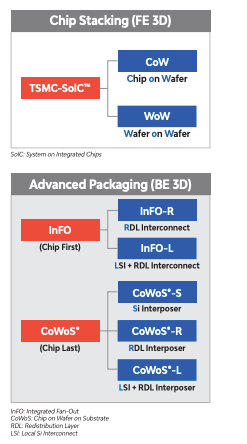
TSMC is showing in their “3D Fabric” concept “Advanced Packaging (BE 3D)” such technologies as integrated fan-out (InFO), a chip first approach with different options such as InFO-R and InFO-L; and chip-on-wafer-on-substrate (CoWoS®), a chip last approach with different options such as CoWoS®-S, CoWoS®-R and CoWoS®-L (Figure 3)
But wait, wouldn’t we expect the names of the large OSAT companies like ASE Group, Amkor Technology, JCET Group, PTI, Tongfu Microelectronic or Tianshui Huatian Microelectronics here? TSMC is a foundry, and that they are strongly involved in advanced packaging is underlining a trend when it comes to WLP.
More IDMs and many foundries are entering into that business taking a share from the OSATs. The reason is easy to understand. Advanced packaging technologies are getting closer to wafer fab processes, using wafer fab equipment, require clean room classes as used in wafer fabs due to the smaller features sizes such as RDL line width, spacing and thickness, via sizes and height, and contact pad pitches. The package is becoming a functional part of the product, chip-package-board co-design and co-development is essential, chip-package-interaction (CPI) considerations are crucial elements.
Looking at the revenues coming from its packaging business, TSMC would be the 4th largest OSAT in the world with an advanced packaging revenue of $2.88B in 2019, and business is continuing to grow. Back in June 2020, TSMC announced plans to invest $10.1B in building a new chip packaging and testing facility in Miaoli, northern Taiwan. The completion of the plant is scheduled for May 2021 with operations set to start in the middle of 2021.
![[err-ad-fallback-title]](http://www.3dincites.com/wp-content/plugins/a3-lazy-load/assets/images/lazy_placeholder.gif)
Emerging packaging technologies are die-to-wafer (D2W) bonding and wafer-to-wafer (W2W) bonding with interconnects formed by thermo-compression bonding (TCB) or hybrid bonding, typically Cu pad to Cu pad without extra interconnect elements. TSMC is calling this in their “3D Fabric” concept “Chip Stacking (FE 3D)” SoIC™ (System-on-Integrated Circuit) with chip-on-wafer (CoW) and wafer-on wafer (WoW).
This recently became a push from the need to disintegrate (de-integrate and break down a large chip into smaller parts) large monolithic SoCs manufactured with the latest wafer fab technology nodes such as 14 nm and below, driven by the digital design into so called chiplets/dielets. These are integrated functional circuit blocks, often reusable IP blocks, that have been specifically designed to work with other similar chiplets to form larger more complex chips inside a SiP. They have been “invented” in the process of disintegration of SoC into many smaller chips for the following two main reasons:
- Process technologies continued to enable higher monolithic integration in one chip, but SoC sizes reached reticle limits, which dictated the maximum size of chip.
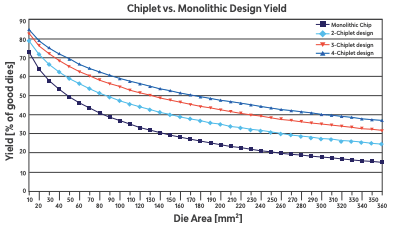
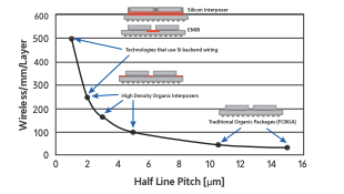
- Economics has resulted in a reversal of that trend due to defect density on large chips directly impacting yield and cost (Figure 4) and significant increased cost for new technology nodes.
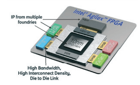
Advanced packaging got the task to enable the rebuilding of the large SoC out of chiplets/dielets targeting the performance of the monolithic SoC or even better, as the functional blocks put together here are manufactured with function optimized wafer fab technologies in different companies with different capabilities, IP ownership, and consequently function specific optimized performance (Figure 5).
Customers can “cherry-pick” to build their own “SoCs” out of the chiplets they consider the best for their applications (Figure 6).
However, there is still a lot of work to do such as standardization of interfaces, and development of the smallest and shortest possible interconnection technologies between the chiplets in the package, often thousands of contacts on a few square millimeters.
Given the trends summarized above and the growth in advanced packaging shown, the equipment supply chain will be under enormous pressure to support the technology development with tailored equipment and process solutions and to meet capacity and productivity requirements once the industry moves into high volume manufacturing.
A key piece of technology is thin film deposition, both on wafer and panel level up to 600mm square substrates.
Thin-film deposition is required to manufacture either seed layers or passivation layers with high uniformity, superior adhesion, lowest resistance, and low particle count. Innovative, flexible, high throughput, highly automated, and high-quality solutions are required by the packaging industry, which in this field are not only OSATs and IDMs anymore, but also foundries as explained above.
Last but not least, physical vapor deposition technology will make it into the printed circuit board (PCB)/ IC substrate industry too, as technology leaders move towards smaller feature sizes too, competing with mainly the traditional Fan-out WLP/PLP players. Embedded trace and molded interconnect substrates e.g. using Ajinomoto build-up films (ABF) are on the rise and present new opportunities for thin film deposition technology leaders like Evatec.
This article originally appeared in Evatac’s newsletter, Layers 6, and is republished with permission.


