AP foundry production to increase by 20x in 2022
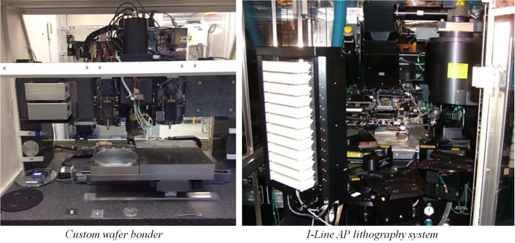
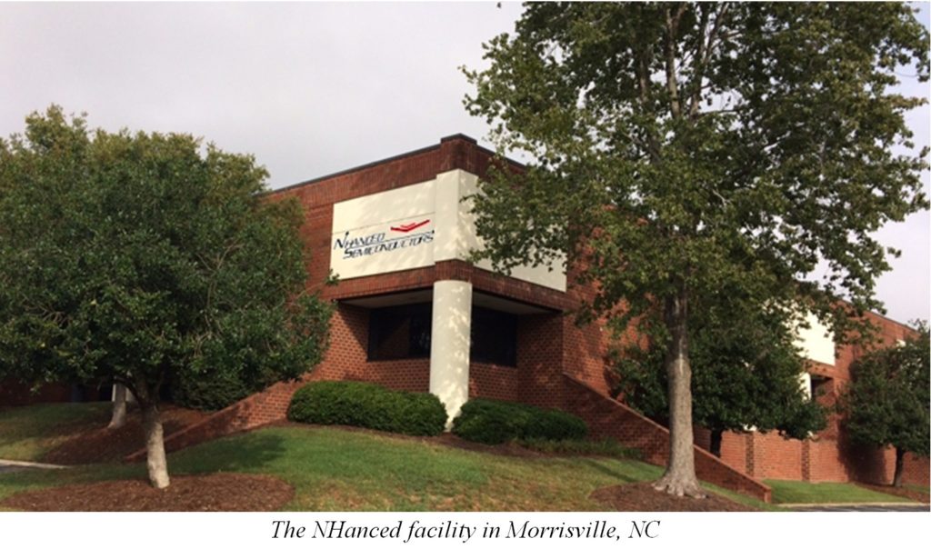
NHanced Semiconductors is expanding the cleanroom of its North Carolina foundry to house a new high-volume line of advanced packaging (AP) equipment. The new line – the first of its kind in the US – will run in parallel with the existing prototyping and low volume production line.

“Demand for advanced packaging is just booming,” states company President Bob Patti. “We’re at an inflection point. Our year-on-year revenue doubled in the first 5 months of 2021; many customers are ramping to volume production.”
The new line is expected to begin production in the second half of 2022, capable of constructing up to 10,000 3DIC wafer stacks per month. The expansion will also enable greater capacity for 2.5D interposer fabrication and die-to-wafer assembly. Domestic sourcing of these AP technologies is critical to aerospace/defense agencies and many US manufacturers.

About NHanced Semiconductors
Headquartered in Illinois, NHanced is a US pure-play advanced packaging (AP) foundry. It specializes in BEoL processing with leading-edge technologies such as photonics, microfluidics, and additive silicon manufacturing. The company’s extensive experience in AP includes die bonding, wafer bonding, extreme wafer thinning, copper and nickel damascene RDL, silicon interposers, chiplets, and micro transfer printing. The fab works with both standard and non-standard substrates, III‑V compound semiconductors, and many specialized materials.


