in this week’s post, we continue our look at the 2020 IEEE ECTC virtual conference.
Siliconware’s presentation “Scalable Chiplet Package Using Fan-out Embedded Bridge (FOEB)” focused on the advantages of its FOEB package for the server, high-performance computing, router, and switcher markets. The difference between today’s 2.5D and FOEB is shown below in cross-section in Figure 1.
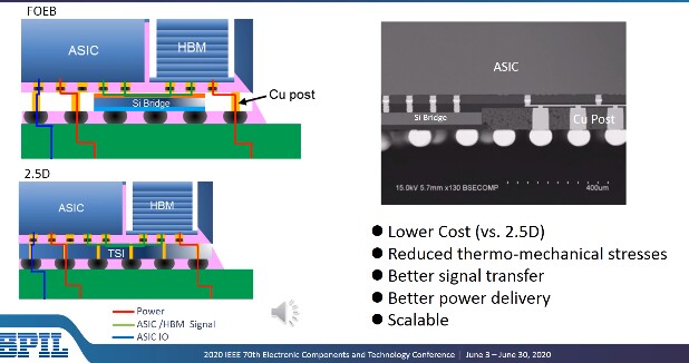
One of the main differences is the copper posts used for power distribution. Further details of the cross-section are shown above in the feature photo.
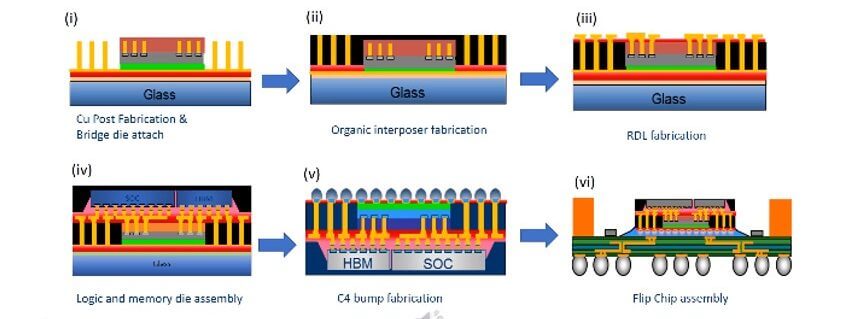
Figure 3 details the process flow as follows:
- Step 1: RDL and copper-post fabrication on glass carrier and bridge die-attach
- Step 2: mold and grind to expose Cu post
- Step 3: RDL layer and microbumps
- Step 4: Place system-on-chip (SoC) die and 4 high bandwidth memory (HBMs) followed by reflow, underfill dispense, and cure. Then second molding is applied to cover the wafer
- Step 5: Removal of the glass carrier, the wafer is planarized and bumped and diced
- Step 6: Diced module is placed onto the organic BGA using conventional flip-chip processing
It is necessary to control the warpage during the fabrication process. Additionally, the mold compound coefficient of thermal expansion (CTE), Tg as well as the glass CTE must be controlled. Based on tests, higher glass CTE is necessary to process this package (Figure 5).
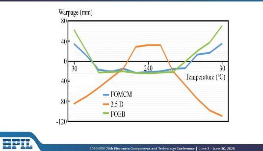
SPIL has concluded that fan out multi-chip modules (FO MCMs) and FOEB have similar warpage and are an improvement on 2.5D packaging approaches.
Figure 5 shows the results of reliability testing.
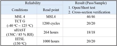
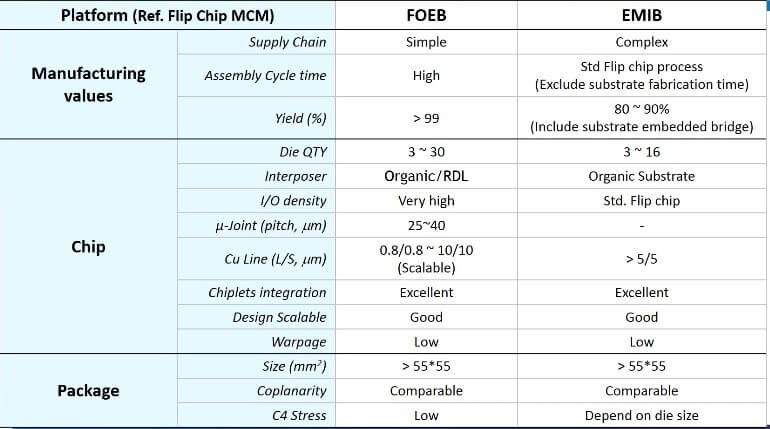
Figure 6 compares FOEB to the Intel EMIB process.
For all the latest in Advanced Packaging stay linked to IFTLE………………………….. Phil


