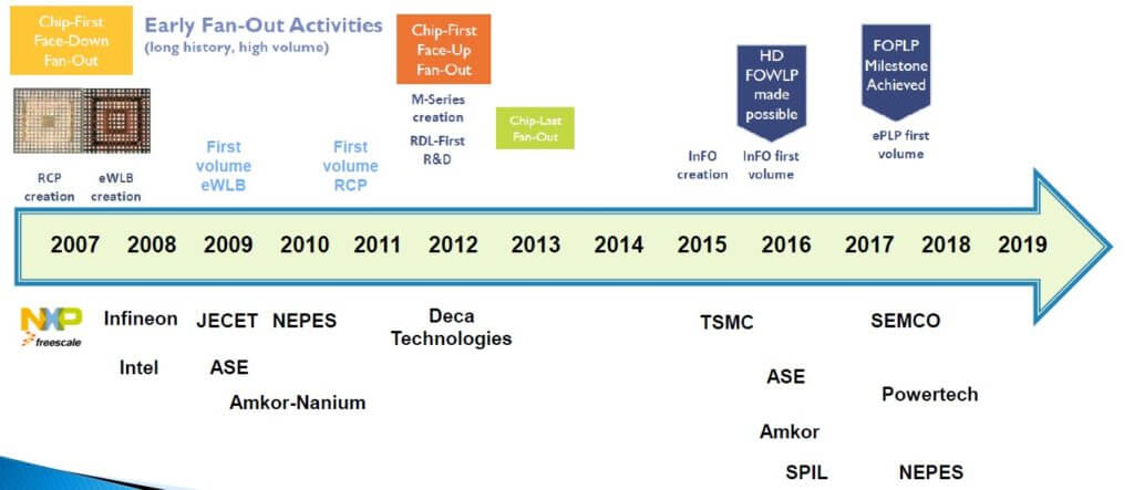
 There are several different fan-out wafer-level packaging (FOWLP) technologies that are currently in high-volume production. The traditional fan-out (FO) technology as initially developed by Motorola and Infineon was a face down, die-first technology that has been in volume production for low-end baseband, PMIC, Codec, Wi-Fi, RF kind of applications since 2008. More recently, die face-up high-density FO packages have been developed such as the TSMC InFO, that has found adoption in mobile phone processor + DRAM package on package format (Figure 1).

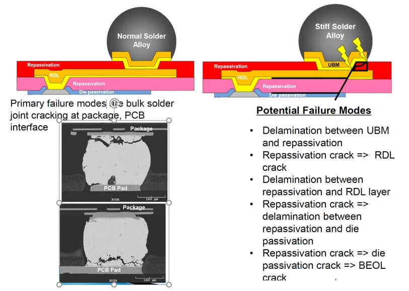
FOWLP has limitations in achieving good board level reliability (BLR) performance. During board level temperature cycling both fan-in and FO wafer-level packages have solder joint cracking as the dominant failure mode. Stiffer solder alloys have been evaluated to minimize solder joint fatigue life, however, the higher stiffness of the solder moves the failure from the solder joint to the package redistribution layer (RDL) trace (Figure 2).

Wafer-level packages for advanced silicon nodes (post 45nm) are also known to have fragile low-k and extremely low-k (ELK) back end of line (BEOL) dielectric layers that can crack or delaminate in cyclic fatigue.
NXP FOWLP Microcontroller
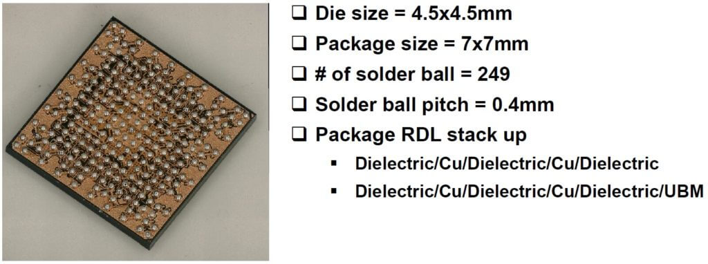
At IWLPC 2019, we learned about a reliable NXP FOWLP microcontroller technology from Gaurav Sharma, Ph.D., NXP Semiconductor. (Figure 3)

Known good die (KGD) were picked and placed active side down on a metal carrier wafer. The die placement and spacing determined by the final FOWLP design. The wafer was then molded and the carrier wafer was removed. This is followed by an RDL and under bump metallization (UBM) processes, respectively. After RDL formation, the molded wafer was back-ground to final package thickness followed by solder ball drop and package singulation into individual units. The package is 7x7mm with 249 solder balls at a 0.4mm solder ball pitch. The solder ball map shows the depopulation of the outermost row as suggested by the results of silicon/package/board co-design. The developed FOWLP had two copper metal redistribution layers (RDL) and 3 dielectric layers.
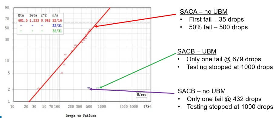
They evaluated multiple dielectric materials and solder alloys but do not identify them or their UBM stack so this information is not very useful to practitioners other than to say that choices are available that pass the following reliability tests.

For the optimized package, Weibul testing showed only 1 fail in 1000 drops in BLR.
For all the latest in Advanced Packaging stay linked to IFTLE……………….


