The keynotes outlined in Part 1 of IMAPS DPC 2017 Covers Range of High-tech Topics, including EDA were obviously very important, but a relatively small part of the entire conference. After the two keynotes on Tuesday morning, I listened to YOLE’s presentation, delivered by Santosh Kumar, and learned that the three big memory vendors (Samsung, Micron, and Hynix) jointly hold over 200 TSV patents in the memory space. Kumar also talked about the importance of TSVs for MEMS integration and back-side illuminated (BSI) image sensors. He showed that interposers with TSVs serve primarily very high complexity, high performance and less cost-sensitive markets, like Networking, Graphics, and Computing. On the other side, the interposer and TSV-less, therefore lower-cost packaging technologies (flip-chip, fan-out wafer level packaging (FOWLP), are gaining significant market share in mobile, wearables and IoT applications.
Hideki Kitada, from Fujitsu’s processor division, showed that single-die SoCs and following Moore’s Law can no longer meet computing market requirements. He outlined how die stacking with TSVs and micro-bumps allows Fujitsu to implement high complexity circuits, manage thermal challenges, and increase yield and reliability by architecting interconnect redundancy into these designs.
SavanSys’ Amy Lujan outlined the process flows for FOWLP and flip-chip, then explained the key factors impacting cost in their model and the assumptions used in this study. Key findings:
- FOWLP is not yet as mature as flip chip, which of course impacts yield.
- Flip chip offers three scrap points – versus only two for FOWLP – and avoids continued processing of bad units better.
- Larger die and package sizes can significantly reduce the number of units per wafer, with it increases FOWLP unit cost.
- Flip chip requires wafer bumping. Larger dies mean fewer units per wafer and a higher “bumping adder” to the unit cost.
Bottom line: Unit cost depends on many variables and SasanSys can help with finding the lowest cost point. (Editor’s Note: Please keep in mind that cost isn’t the only criteria. Evaluate also thermal performance, the impact of parasitic capacitance and inductance on electrical performance, the value of potential board space savings, minimum contact spacing of the PCBs to be used, package height allowed, etc…)
Aric Shorey from Corning presented the benefits of glass interposers for packaging IoT, mobile, medical and other solutions. He pointed out key reasons for using glass as a carrier during manufacturing or in wafer or panel-form in a manufacturing flow. Shorey listed a number of companies using glass today and explained why:
- 5G phones and Lidar units in automotive use it, because of the extremely low insertion loss (a.k.a. loss tangent) at or above 60 GHz is essential.
- An adjustable coefficient of thermal expansion (CTE) minimizes warpage and yield-loss.
- Mechanical stiffness and chemical resistivity make glass well suited for rough environments.
- Glass can be manufactured in almost any thickness, in several wafer sizes and any x-y panel size can be now quickly and cleanly drilled with laser pulses.
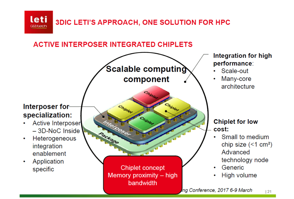
Severine Cheramy presented Leti’s accomplishments and roadmap for high-density designs. She started her presentation with a very compelling statement: Smaller form factor improves performance per Watt, latency, and bandwidth between processor and memory. Then Cheremy outlined Leti’s R & D focus on 3D TSV, BSI image sensors, and 3D monolithic (a.k.a. CoolCubeTM) technology. She used several slides to highlight the benefits of direct bonding (wafer-to-wafer and die-to-wafer). Like many speakers from Leti at other conferences, Cheramy explained how they managed to develop a much lower temperature logic process, to allow adding a second layer of circuitry to a wafer, without significantly changing transistor performance in the first layer. This low-temperate process is essential for combining two (and eventually more) layers of circuitry in a CoolCube. For me, the most promising and immediately deployable technology at Leti is their work on high-performance solutions combining die-lets (a.k.a. chiplets) on one or more interposers. See Fig. 1 below.
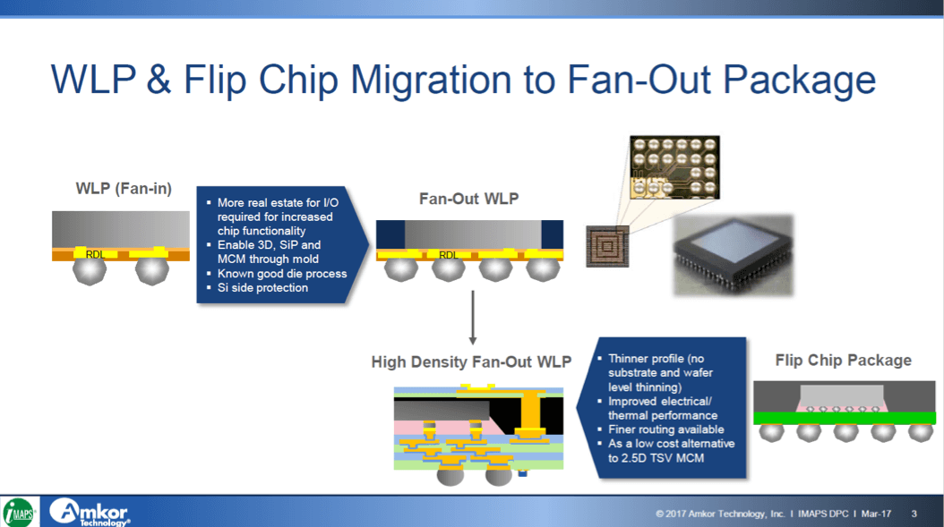
Amkor’s Curtis Zwenger talked about migrating flip chip designs and/or fan-in packages to a single or multi-die FOWLP. See steps and benefits in Figure 2. Zwenger emphasized that Amkor’s SWIFTTM packages can be as thin as 0.4 mm, a key differentiator in smartphones and other mobile applications. He also mentioned that SWIFT packaging demonstrated 11% better power integrity (PI) as well as significantly better thermal performance versus an equivalent flip-chip solution. Zwenger also announced that Amkor will offer multi-die SWIFT packages in 2017 and introduce such packages uses low-cost laminate substrates in 2018.
Seung Wook Yoon from STATSChipPAC (now part of JCET) presented their broad offering of system-in-package (SiP) solutions and emphasized the many benefits of the production-proven embedded wafer level ball grid array (eWLB) package, including: <0.3 mm thin, 5/5 micron proven and 2/2 micron l/s in development. He also highlighted the ability and benefits of embedded passives and mentioned that on-chip inductors can achieve only 20 to 25 quality factor while as integrated passive devices (IPDs) they show a Q of 35 to 40, and reduce power dissipation significantly.
Steffen Kroehnert from Nanium ( soon to become part of Amkor ) focused on integrating MEMS and sensors in eWLB packages. He projected a very bright future for eWLB technology. It was invented by Infineon and licensed by Nanium, ASE, and STATSChipPAC. Kroehnert stressed that integration of MEMS and sensors adds a lot to the complexity to IC test and requires special packaging to keep moisture and other environmental factors from impacting the performance of these devices. He also wanted us to know that to date Nanium shipped more than 1 Billion ICs in eWLB packages.
The Global Business Council
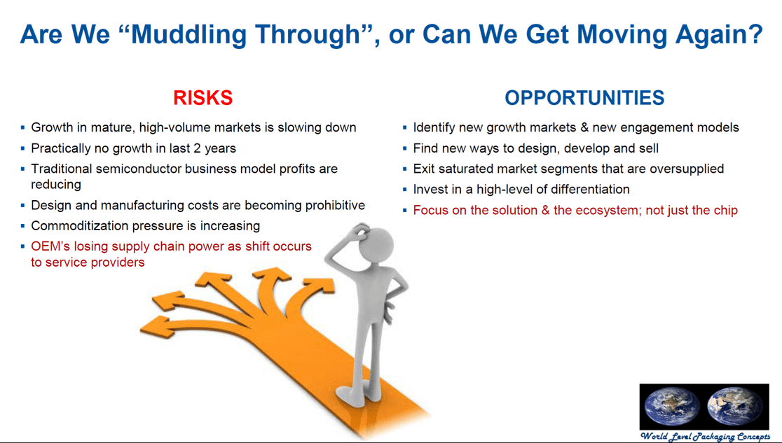
On Wednesday morning, Jim Walker, formerly packaging guru at Gartner, now president of World Level Packaging Concepts (WLPC), emphasized in his keynote multiple times that “business as usual” is no longer an option for success. The many changes in market requirements and, in response, lots of new semiconductor design and manufacturing technologies, demand major changes at all levels of the supply chain to remain successful. See some of his observations and suggestions in Figure 3.
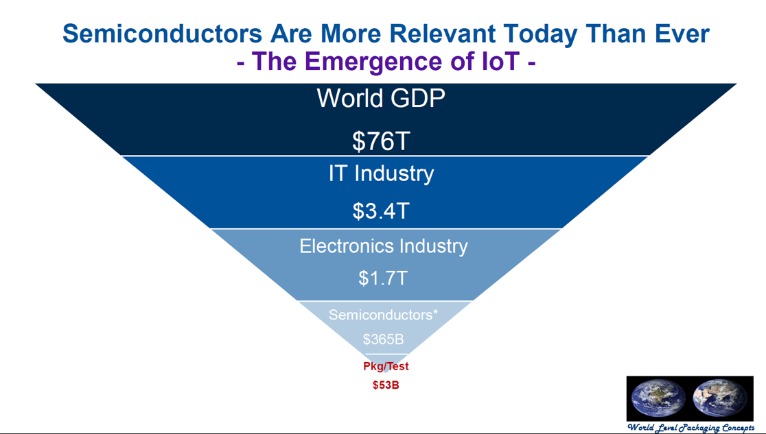
I also like Walker’s slide showing how dependent the large world economy is on the small IC packaging and test segment. It also confirms how much the semiconductor industry could increase revenues by “moving to the system-level of the electronics industry” and capturing part of their value creation – see Figure 4. Walker also pointed out that traditional system companies are moving to designing their own semiconductors, that electronic manufacturing services (EMS) and original design manufacturers (ODMs) companies will vertically integrate down – e.g. Foxconn trying to buy Toshiba’s memory IC business. This shows how the IC value creation is shifting to advanced packages. Last, but not least, Walker pointed out that the M&A wave will continue across the entire semiconductor supply chain, including packaging, but can’t be the only way to strengthen and grow our industry.
Jan Vardaman from TechSearch International gave the second market research presentation and got the audience’s full attention by telling us about her daughter’s recent and severe car accident. Thanks to PASSIVE safety, the daughter was not badly hurt. As all our minds were tuned to hear from Vardaman about ACTIVE safety, she started to talk about the very rapidly growing automotive electronics segment. She predicted that cars will soon have 10 to 20 cameras – each one using vertical die-stacking – lots of sensors as well as sufficient processing power to keep the passengers – and in the near future also the still needed driver – save. See an example in Figure 5.
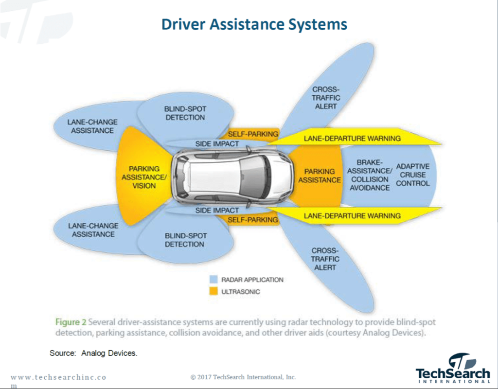
Vardaman pointed out that security (protecting car and passengers from outside forces) and Safety (protecting the outside and passengers from the car) are major criteria for automotive applications. Unlike mobile devices, we may simply discard, especially if they fail after a few months already, automotive electronics needs to prove reliable for more than a decade and operate reliably across a wide temperature range of – 50 up to + 175 oC. High levels of integration, such as system-in-package (SiP) solutions will be needed to minimize failure-prone interconnects, increase performance per Watt, minimize form factor and simplify customization. Vardaman projected that by 2030 the electronics content will add up to about 50% of a car’s cost. Like several other speakers at the conference, she pointed out that die-package-board- system CO-design is needed to create cost-effective and reliable solutions for self-parking and self-driving cars.
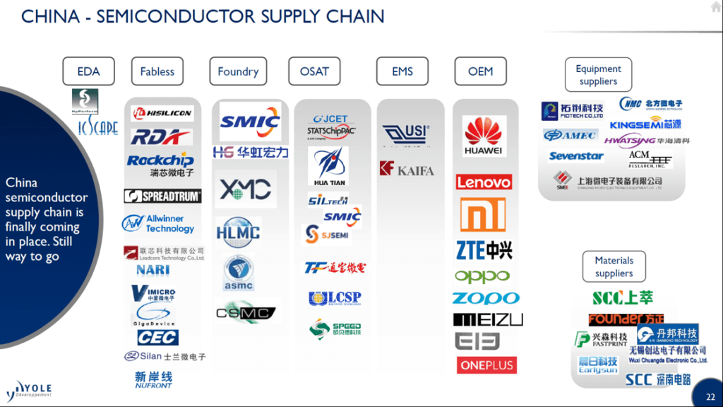
Santosh Kumar from YOLE was the third market analyst to present. He focused on wafer bumping and IC packaging capabilities in China talked about the rapidly increasing number of fabless IC vendors and the expanding and maturing semiconductor EcoSystem in China. See Figure 6.
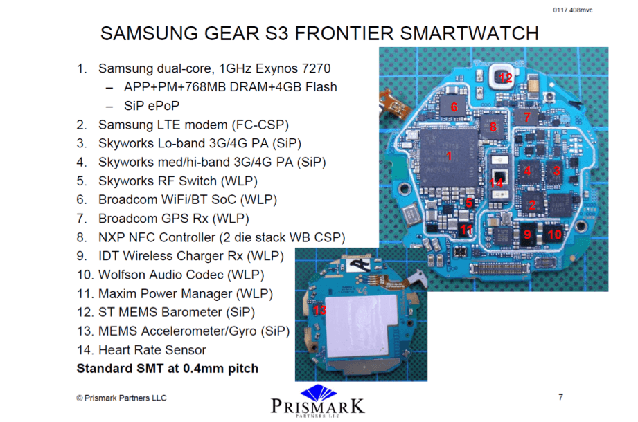
Brandon Prior from Prismark Partners talked about the changing landscape in the back end and emphasized that advanced packaging technologies are essential to capture opportunities in the mobile, wearables and IoT markets. He showed a picture of the Samsung S3 smartwatch assembly and pointed out how many companies are needed to supply state of the art ICs, sensors and passives and assemble all these components into a system. See Figure 7. Prior confirmed other speaker’s comments about the large investments needed to establish an advanced packaging line with a hard number: TSMC invested already $ 800 Million in package development, capital equipment, and manufacturing flows.
High-quality packaging materials are also essential for the success and rapid growth of advanced packaging technologies. Rosalia Beica and Eric Huenger demonstrated clearly that they know what’s expected from them and conveyed Dow Chemical’s capabilities and ongoing efforts to meet these diverse market requirements for substrates and other packaging materials.
 Due to meetings with customers and other work to keep my company going, I was not able to attend other presentations at this impressive conference. Also, as my body can only be in one place at a time, I had to pick just one out of the three parallel sessions. Just in case you are wondering how people can digest such a flood of information, let me tell you: There was also some fun, relaxation, very good food and even native music at the Wednesday barbecue. The full program is here.
In case you had to miss this IMAPS conference in early March, and want to know how advanced technologies can help differentiating your products and/or services, please consider attending one of iMAPS’ next conferences.
Thanks for working your way through this extra-long blog! I am looking forward to your feedback …Herb


