The 2016 International Wafer-Level Packaging Conference (IWLPC), which took place October 18-20, 2016 in San Jose, CA, focused on a theme of “Bridging the Interconnect Gap”, as the industry faces new challenges due to the onslaught of Big Data brought about by the Internet of Things (IoT). To provide vision on how best to address these challenges using advanced packaging technologies, the IWLPC organizing committee turned to industry research and development experts, inviting Prof. Klaus-Dieter Lang, Fraunhofer IZM; and Prof. Rao Tummala, Georgia Institute of Technology, to deliver the keynotes for this year’s conference.

Lang talked about how these challenges can be solved by evolving smart systems into cyber-physical systems that will connect with the networks to improve latency times. He also provided some examples of Fraunhofer IZM’s work in developing these systems and technologies to support them, such as efforts to optimize through silicon vias (TSVs).
While two years ago we thought it would be sufficient to transmit data from a sensor to the cloud and wait for decisions to come back, we now understand that this isn’t possible, he said. This is because the IoT is changing the way we think about communications. “We used to say the new communication systems will be part of our car. Now we say our car will be part of our communication systems,” said Lang. To realize this level of connectivity requires thinking from the system side.
“If we want to have a decision or reaction in a working space, we need that information now, not an hour from now or tomorrow,” added Lang. As such, cyber-physical systems need to deliver immediate reactions by integrating the data processing with the sensor in the same system. Additionally, more than just the technology needs to be considered. Sensing, data processing, security of that data, power supply, and increasing operations frequencies to 60Ghz all must be considered to realize these smart systems.
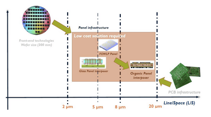
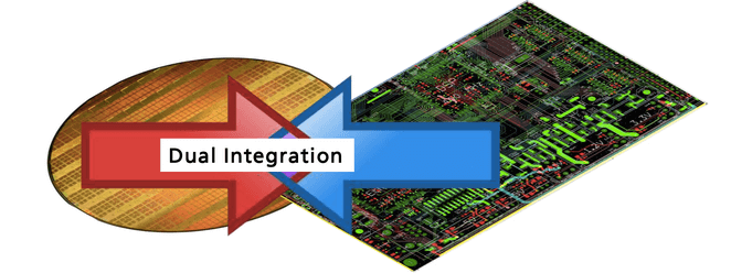
Lang said an advanced integration strategy to achieve this focuses on the fusion of system-on-chip (SoC), wafer-level packaging (WLP), panel-level packaging (PLP), printed circuit boards (PCB), flexible substrates, 3D integration and system packaging to achieve dual integration (Figure 2). For example, finer lines and spaces can be achieved by combining semiconductor and PCB processes like embedding bare die into organic substrates or leveraging interposer technologies using PCBs, glass, and silicon. Wafer and panel-level molding are also critical for fan-out wafer level packaging (FOWLP) and FOPLP.

Tummala’s talk focused more specifically on the gaps that can be filled by FOWLP and FOPLP including the interconnect, thermal, power, reliability and cost gaps, and how Georgia Tech is working to close the gaps. Contrary to what was discussed during the FOPLP panel discussion, Tummala is of the mind that FOPLP is emerging to address issues of FOWLP.
He concurred with Lang that the end goal is to make a subsystem, and said this requires us to go to large panel formats, particularly when the system calls for large body multi-chip modules (MCMs) and system-in-package (SiP). “According to the panel discussion, FOPLP is not shaping up as well as I see it,” said Tummala. “Panel is happening. Five years ago it was a debate, but it is now happening.”
While he admitted his definition of FOPLP may be broader than others, Tummala cited examples of FOPLP happening now at Imberra, AT&S, and Fraunhofer IZM. He said ASE offers advanced embedded assembly in panels, and that SPIL and PTI offer panelized fan-out and panelized molded fan-out, respectively. J-Devices offers a wide strip fan-out, and ASE has advanced embedded assembly uses a chips-last approach. Deca Technologies offers a face-up fan-out package. On the power semiconductor side, Schweizer’s p2 pack power embedding uses large panel formats.
At Georgia Tech, Tummala is touting a chip-last approach in a laminate panel, calling it “chips-last with chips-first benefits.” He’s also really enthusiastic about the research institute’s work using glass as the substrate, dubbed glass fan-out (GFO), because it can support the same features sizes for lines and vias as silicon, at a package-level cost, and behaves like silicon in back-end-of-line processes. In comparison with laminate, it achieves 2µm l/s vs. 6µm and 10µm vias. He said in panel format, glass offers a 5x cost reduction that can increase to 10x for ultra-large formats.
While traditionally, the packaging approach was driven by what was the lowest cost to achieve the required performance, Lang noted that in systems of tomorrow, the priorities of miniaturized smartness, cost, and performance will change based on the end-use application.
As such, we can expect miniaturized smartness to drive the automotive, medical, Industrie 4.0 and robotics applications. The cost will drive wearables and IoT devices, and performance will drive mobile wireless and power module applications, thus providing an opportunity for all levels of development in the advanced packaging space. ~ FvT
PS: For more on IWLPC, read Reflections of IWLPC 2016.


