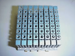
 There’s probably no more fitting venue for discussing future directions for processing and packaging technology in integrated circuit fabrication than the Computer History Museum in Mountain View, CA. After all, “The mission of the Computer History Museum is to preserve and present for posterity the artifacts and stories of the information age. As such, the Museum plays a unique role in the history of the computing revolution and its worldwide impact on the human experience.”
“What’s past is prologue,” right? “The child is father of the man.” Or at least that’s how the English poets (Shakespeare, Wordsworth) would have us see it.
Computer history was our launch pad for the 2013 GSA Silicon Summit, which recognized in its mission statement that “Moore’s Law has transcended computing expectations; however, its promise will eventually reach scalability limitations due to extraordinary consumer demands. Future technology encompasses breakthroughs capable of interaction with the outside world, which the More than Moore movement achieves. Through integrating functionalities that do not scale to deliver cost-optimized and value-added system solutions, this trend holds significant potential for the industry. This event will explore the business and technical factors defining the More than Moore movement, and address how it will yield revolutionary electronic devices.”
I always think of the phrase “More than Moore” as being a kind of code that needs decoding or deciphering. “What does ‘More than Moore’ mean?” I might ask you, and you might then respond “What does ‘More than Moore’ mean to you?”
So inspired by computer history, and powered by Google, I set out to find a better answer to the More than Moore question and found this: “Since the early 70’s, the semiconductor industry’s ability to follow Moore’s law has been the engine of a virtuous cycle: through transistor scaling, one obtains a better performance–to- cost ratio of products, which induces an exponential growth of the semiconductor market. … The industry is now faced with the increasing importance of a new trend, ‘More than Moore’ (MtM), where added value to devices is provided by incorporating functionalities that do not necessarily scale according to ‘Moore’s Law’”. (Source: More-than-Moore White Paper, ITRS, 2010. Italics: mine.)
There’s also this, again from the ITRS 2010 White Paper: “The ‘More-than-Moore’ approach typically allows for the non-digital functionalities (e.g., RF communication, power control, passive components, sensors, actuators) to migrate from the system board level into a particular package-level (SiP) or chip-level (SoC) implementation. … The objective of ‘More-than-Moore’ is to extend the use of the silicon-based technology developed in the microelectronics industry to provide new, non-digital functionalities. It often leverages the scaling capabilities derived from the ‘More Moore’ developments to incorporate digital and non-digital functionality into compact systems.”
And what might the viable commercial prospects be for deploying ‘More than Moore’ technology?
If you’re someone who likes to follow the money (and not just the technology), then, according to the ITRS paper, the MtM money flows from here: “Underlying the evolution of markets and applications, and therefore their economic potential, is their potential in addressing societal trends and challenges for the next decades. Societal trends can be grouped as health and wellness, transport and mobility, security and safety, energy and environment, communication and e-society (this latter term including infotainment).”
The MtM money might even begin flowing from the Internet of Things (IoT).
In a format I would like to see more of at events like this, the GSA Silicon Summit makers-of-opening-remarks turned the helm over, in order, to three well prepared moderators, who led actual conversations with three sets of distinguished panelists without allowing the panelists to resort to PowerPoint slidedecks of their own. This was pure conversation — not the (too) usual present, posture, and feint — with some time allowed for audience questions.
The day was divided into three sessions. Session One, Disruptive Innovation – Enabling Technology for the Connected World of Tomorrow, moderated by Dan Rabinovitsi, Qualcomm, featured panelists from IBM, Freescale, Peregrine, Open-Silicon, and Rambus. Panelists during Session Two, How More than Moore Impacts the Internet of Things, represented Tensilica, ARM, Cisco, and STMIcro. The session was moderated by Ed Sperling, System-Level Design. And Session Three, Integration Challenges and Opportunities, moderated by Bruce Kleinman, GlobalFoundries, comprised panelists from Microsemi, Altera, ASE, Soitec, and SuVolta.
With “More than Moore” as the code phrase of the day, I kept my ear to the ground for decoded responses from the GSA Silicon Summit panelists and moderators, and also from some of the exhibitors and attendees present during the mingle and mix portions of the schedule. I heard such significant tidbits as:
“It’s natural for MEMS and mixed-signal devices, or MEMS and logic devices, to live in a side-by-side (2.5D) world.”
“Organic substrates for 2.5D interposers show great promise for reducing 2.5D interposer costs – look particularly to the work being done by Georgia Tech.”
“If you don’t follow scientific change then what you practice reverts to witchcraft.” (The Rabinovitsi Paradigm.)
“Innovation in packaging may be more relevant than Moore’s Law moving forward.”
“3D packaging is becoming a very exciting technology, with as much relevance as a process node shift.”
“The IoT needs packaging innovations – not Moore’s Law technology progression.”
“FinFET or packaging – where’s the smart money playing? The problem is one of die / device performance versus system performance – and packaging drives system performance.”
“That being said, 3D packaging is not a panacea – basic economics still rule.”
“Seven years from now it will be IoT applications driving the industry – and Moore’s Law progress doesn’t apply to the analog world, hence the need to work on heterogeneous integration / 2.5D / 3D IC.”
“New generations of network-side IC products are only 15% innovation – the other 85% is composed of standard I/O and memory IP. Moving some of that 85% from the board to the interposer or to a 3D stack will be a huge performance improvement – 3D memory integration, for example, is positively disruptive.”
“But doesn’t CMOS integration always win? Monolithic integration, or heterogeneous integration using 2.5D / 3D IC; either way it comes together, no one size fits all.”
“The 28nm process node has a lot to like about it: speed, cost, High Volume Manufacturing (HVM) capability, and IP portability all look good compared to 14nm FinFET.”
“Challenges that need addressing in 2.5D / 3D IC are supply chain related. The current cost structure for 2.5D / 3D is leveraged by materials and processing equipment.”
“Do we currently even have a functioning 3D IC ecosystem?”
“Thermal challenges have kept 3D IC from coming to the mainstream. 2.5D is much better than 3D from a thermal perspective.”
“As for testing 2.5D products, it’s not that different from the testing IBM did for its Multi-Chip Module products. That sounds easy, it’s not, but it does show how you can test, and ship, these products to customers with confidence.”
 My take: those comments make for a nifty real-world overlap with the 2010 ITRS white paper on More than Moore, and are a pretty much spot-on reflection of how the Global Semiconductor Alliance promoted the Silicon Summit, as a venue to “… explore the business and technical factors defining the More than Moore movement.”
Computer history in the making, made where computer history resides. The virtuous silicon cycle continues, with a boost from 2.5 / 3D IC. From Petaluma, CA, thanks for reading. ~ PFW


