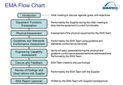
Last week, SEMATECH and ISMI announced they would be conducting Equipment Maturity Assessments (EMAs) of several critical 3D tools during 2012 to establish functional equipment capabilities and address high volume manufacturing (HVM) maturity issues for 3D IC manufacturing. This is a significant step in SEMATECH’s goal to accelerate the 3D technology revolution. To find out more about this, I talked with Sitaram Arkalgud, director of the 3D program at SEMATECH, and Lorn Christal, project manager at ISMI, about the EMA process, and how this focused assessment of tools, development systems, processes, and materials will help identify and plug the gaps to pave the way for HVM of 3D devices.
“We are at the point where 2.5D products are coming out this quarter, and 3D products are following close behind next year. It’s more real than it’s ever been before,” explains Arkalgud. “I see these first products as pipe cleaners. Once they get through and we see them being used, the floodgates will open.” At that point in time, he notes, it will be critical for the industry to be prepared for HVM.
While front-end (foundry) and back-end (packaging) tools are all ready for HVM, the in-between processes that involve the backside — such as temporary bonding and debonding, wafer thinning, RDL, wafer or die bonding and wafer release — are still fairly immature when it comes to HVM readiness. Safety specifications, software interfaces, process specifications, materials, and equipment standards still need to be defined. Arkalgud says EMAs can provide the play book to determine the issues and help suppliers fill in the gaps.

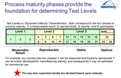
Christal explained that EMA methodologies can be applied to virtually any equipment — from a FOUP to a EUV tool — to determine the equipment’s current level of maturity versus its expectations. “It helps suppliers understand what they must do to ensure equipment meets expectations in a timely manner,” he explained. “The EMA provides valuable focus on the standards, performance levels, and regulatory requirements for high-volume manufacturing.”

EMAs are not new; they’ve been successfully used during wafer transitions, and are beneficial to companies who want to understand requirements for HVM, and need to improve their systems, equipment development and engineering controls. “It’s one thing to have mature equipment, it’s another to improve upon that maturity via robust development procedures,” noted Christal.
It’s important to note that SEMATECH doesn’t see itself as in the ratings business. Christal explained the goal of this program is not to designate one company’s tool as a better than another, but rather assess the participating tools’ maturity and point out where improvements can be made. It’s a service to suppliers rather than a report card to manufacturers. Suppliers who participate are likely to see an improved time-to-market because they understand what is required. EMA methodology is a focused, structured process.
Arkalgud says EMAs are particularly beneficial to smaller companies entering the market with tools targeting this new area. Large companies have internal processes established and may not need to have ISMI conduct EMAs. Additionally, companies established in the packaging end of the market are facing new requirements long held in front-end processes; such as smaller feature sizes. EMAs help companies understand what these requirements and expectations are, and what it means to play in the front-end market.
Both Arkalgud and Christal agreed that while this EMA process is primarily focused on equipment, it can also be applied to materials and processes, and would be useful in the feasibility stage of materials development. It can also be extended to design tools, and test and inspection equipment.
Ultimately, the goal of SEMATECH and ISMI is to help members develop processes and materials to reduce costs and maximize their return on investment as 3D process approach HVM. To learn more about conducting EMAs for suppliers of wafer backside processing equipment, contact 3DInterconnect@sematech.org. ~ F.v.T.


