


I just got back from the IWLPC 2011 in Santa Clara, and my head is full of commentary just begging to be dumped on a page. This year’s agenda was jam packed with 3D discussion — plenary talks by Matt Nowak of Qualcomm and John Lau of ITRI, a panel on 3D infrastructure, and the 2.5D/3D debate — which was great for me and the rest of the 3D InCites community, but I kind of felt bad for the MEMS and WLP folks, because beyond technology tracks devoted to MEMS and WLP, most of the ‘extra’ events focused in the 3D technology space. But then again, I guess 3D really does touch on MEMS and WLP as well, so maybe it’s just indicative of the direction the semiconductor world is going.
As always, I gathered enough material for several posts, so you can look forward to some in-depth articles in the next week or so. But while they’re still fresh in my mind, I want to share some of those particularly A-Ha! moments I always have when I’m in the presence of semiconductor greatness.
On the broad 3D scope, we’re still talking about a lot of the same things we always talk about: remaining technologies, supply chain issues, IP concerns, who will own the problems, and even whether or not 3D will EVER happen (although the naysayers seem to be dwindling). The changes to these discussions are sometimes subtle, and it’s a trick to tune out the rhetoric and find those notable moments. Most of those come from off-the-cuff comments during the panel discussions, rather than the prepared presentations.
The 3D infrastructure panel discussion was challenge-heavy and solution-light – because the jury is still out on the solutions. I posed the question – any ideas what’s needed to solve these issues? Jan Vardaman, TechSearch Internationsl, got right to the point. “MONEY.” Yep – she’s right. We can speculate all we want about these things and offer up opinions, but it’s ALWAYS about the bottom line. Just as that feeling of frustration was setting in, Sesh Ramaswami, of Applied Material said his company is getting ready for pilot production of 3D ICs, and the focus is changing from “development” to “production”. He also explained that although it might seem that solutions aren’t being found to the infrastructure issues, in reality there’s stuff happening all over the place very fast, it’s just not being shared here, that’s all. Ok. Good to know.
The sparring match between Ramaswami and Vardaman on the ease of manufacturing silicon interposers was one of the most entertaining elements of the panel discussion; really of the whole event. It started when Ramaswami responded to the “what will be the first product out” question, expressing the desire for it to be silicon interposers with TSV (I think that’s already happening, isn’t it?) His reasoning? “It’s simple to make, and we can learn a lot from it. It’s a cheap way of learning.” He even went so far as to say the price charged for TSV silicon interposers was too high for what it delivers. Vardaman begged to differ, citing TSMC’s Douglas C-H Yu’s presentation at SEMICON West, who talked about the difficulties of putting down two RDL layers on a wafer to create silicon interposers. John Lau came to Ramaswami’s defense, agreeing that silicon interposers are easy to make and citing his own success with interposer RDLs. Vardaman challenged with “I’d like to see the yields on that.” To which Lau retorted “It’s not fair to ask a researcher about yields!” That brought the house down.
I’d say Game, Set and Match to Vardaman on that one.Yields are right up there with the cost as the potential 3D deal breaker. According to John Lau, 3D integration’s feasibility was proven back in 1986. It didn’t make it to production then for the same reasons its been draggin ever since. Cost. What’s different now is the lack of any other way to meet performance and power requirements for today’s applications.
One a-ha moment came from the audience. “EMS providers have figured out how to handle similar supply chain logistics issues with electronics assembly. Why doesn’t the semiconductor industry adopt a similar model for the 3D IC infrastructure?” A collective “good idea!” rippled around the room and my own head spun around to see who had offered up this nugget of brilliance. It was Alec Barbiarz, director of new business development for Nordson Corp. Ron Leckie, infrastructure consultant, agreed that the model is good, but would be trickier for the 3D market due to handling issues and test- both of which are ‘orders of magnitude’ more difficult when you can’t touch, hold or handle a part. At the very least, adopting lessons learned by the EMS supply chain could help in figuring out our own.
Throughout the even — beginning day one with Fraunhofer EMFT’s Peter Ramm’s question to Matt Nowack, through to the Thursday afternoon panel formed to entertain that very topic — the 2.5D vs. 3D debate carried on. Nowack’s assessment was that 2.5D and 3D will progress in parallel and go on in parallel because the technologies address different needs. Different markets will be drive different requirements. (After that response, I wasn’t sure we even needed the panel because it summed it up quite nicely.) Andre Rouzad, of CEA-Leti, put a similar spin using different words: 2.5D and 3D may be evolutionary cousins, but 2.5D doesn’t necessarily lead to 3D. And while he maintains that 2.5D and 3D technologies will coexist, panelist Phil Marcoux, principal PPM, strongly favors the 2.5D approach. Due to technological and logistical reasons such as keep out area requirements; performance impact on the IC due to TSV proximity; high cost; and impact on infrastructure, 3D TSVs are not ready for prime time. Its’ too revolutionary, where as 2.5D is evolutionary, is suited to mixed interconnect ICs, and is not limited to silicon as a substrate material.

With the caveat that 3D SILICON (not interposer, and not 3D IC) will ultimately be the way to go but is unlikely to happen until 2020; John Lau expressed that in the interim, passive interposers for 3D integration is the most cost effective solution, because it avoids ‘digging holes’ in the active ICs. The difference between 2.5D and 3D with passive interposers, is that 2.5D only puts active die on one side of the interposer. In a 3D interposer configuration, as both Lau and Georgia Tech’s, Rao Tummala demonstrated, puts a memory stack on the top of the interposer and a logic die on the other. The difference between Lau’s work and Tummala’s, is that Tummala’s can also be achieved using glass interposers; which he says brings the cost down even further. Tummala has 27 partner companies working with him at Georgia Tech to bring this to market. According to both Scott Jewler of Powertech and Ron Huemoeller, of Amkor, while customers aren’t asking for glass interposers, and therefore the companies aren’t mobilized to work with glass, they are open to the concept and could accommodate the needs if asked.
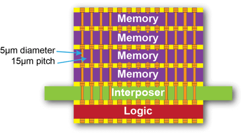 Figure: 3D Silicon Interposer with Memory Stack and Logic Chip. (Courtesy of PRC)
Another zinger came from John Lau, who asked Huemoeller why Amkor isn’t creating and filling TSVs today while Powertech, ASE, STATS ChipPAC and SPIL have all added capacity to do so. Huemoeller explained Amkor’s strategy- they don’t invest in a platform until they know it’s going to stick. They’ve invested in TSVs insofar as they have a complete set of 300mm (& 200mm) tooling in place to support TSV product development / growth. There are customers with programs in place for both 3D IC and 2.5 interposer stacking logic on interposer and logic and memory on interposers. He thinks 2.5D and 3D will coexist nicely, and starting off with 2.5D allows the kinks to be ironed out of 3D. Huemoeller’s overall point; once a platform has been developed and qualified in, it stays. So at Amkor, 2.5D is firmly in. You can take that one to the bank.
Powertech’s roadmap is slightly different because their core technology is DRAM. Jewler reports that PTI has installed and is at various stages of development with fully automated volume manufacturing tools for TSV via last and middle middle-end-of-line (MEOL) processes, 3DIC Die Stacking, and Silicon Interposer Assembly. 2.5 D and 3D will coexist, he notes, and reminded us all that 3D IC memory stacks will be part of the interposer configuration. Therefore, PTI will be production ready for TSV 4 die memory cube manufacturing in Q1, 2012
At the end of the day – I’m thinking the consensus was that 2.5D and 3D will coexist. DRAM stacks will be 3D IC most definitely. Otherwise, “digging holes” as John Lau likes to phrase it, in active die, is a bad idea. Passive interposers for 2.5D an 3D are a more cost effective and viable solution.
On the other hand, while we all continue to debate the issue, there’s likely to be somebody out there getting it done. Maybe at the end of the day, we’ll all just be surprised. ~ F.v.T.


