Evatec delivers first CLUSTERLINE® 310 for Advanced Packaging on small panel formatsOct 13, 2026Evatec has delivered its first dedicated CLUSTERLINE® 310 for panel...
Heraeus Electronics Webinar: What materials perform when failure is not an option?Oct 08, 2026Link to Register As automotive, aerospace and defense, industrial, and...
Rapidus Unveils “Rapidus CORE”, New Global Ecosystem Framework Supporting the Development and Mass Production of Cutting-Edge SemiconductorsOct 06, 2026As part of its first phase, Rapidus is announcing the...
Applied Materials and KIOXIA Partner at the EPIC Center to Advance Next-Generation Memory TechnologySep 30, 2026Companies will collaborate to develop advanced memory structures, chip stacking...
Toray Develops Industry-First Technology to Recover PPS from Waste MaterialsSep 30, 2026Toray Industries, Inc., announced today that it has developed what...
DBC vs. AMB vs. Thick Film – Choosing the Right Ceramic Platform Oct 15, 2026 · By Remtec, Inc. · 3D In-Depth, Processes and Technology
Why Hybrid Bonding Is Hard to Perfect Oct 14, 2026 · By Chad Wallace · 3D In-Depth, Design, Processes and Technology
Beyond the Grating: Rethinking High-Power Semiconductor Laser Reliability for AI Datacenter Optics Oct 08, 2026 · By Akshitha Gadde · 3D In-Depth, Processes and Technology, R&D and Collaboration
Open-Cavity Plastic Packages: A Practical Approach to IC PrototypingOct 09, 2026Developing a new IC involves more than designing and fabricating...
Why Optical High-Volume Test is 10x More Challenging than Electrical High-Volume Test At the Si-Photonics Packaging Summit 2026Oct 07, 2026Unlike electrical testing for semiconductors, automating optical test is extremely...
Can Embedded Passives Fix AI’s Power Delivery Problem?Oct 06, 2026What you’ll learn: Where are the real power “bottlenecks” in...
Overcoming Cleaning and Plating Challenges in Panel-Level Packaging and ManufacturingSep 30, 2026Advances in automotive, high-performance computing (HPC), artificial intelligence (AI) and...
Halftone Photomasks for Next-Generation DisplaysSep 30, 2026Modern flat-panel displays depend on highly complex multilayer structures fabricated...
Siemens and TSMC advance AI-powered Semiconductor Design AutomationSep 23, 2026Siemens’ EDA portfolio supports TSMC advanced process technologies, TSMC 3DFabric®...
Inside Siemens Electronics Factory Erlangen | AI, Robotics & the Industrial Metaverse in ActionOct 13, 2026
See What the IMAPS 59th Symposium on Microelectronics Exhibit Hall Has in Store!Sep 18, 2026Thank you to our valued IMAPS exhibitors for your continued...
IMAPS 59th International Symposium on Microelectronics: Technical Program and Exhibition Focused on Intelligent Packaging for the AI Era (Heterogeneous Integration & Photonics)Sep 18, 2026The International Microelectronics Assembly and Packaging Society (IMAPS) will host...
Tackling the Memory Wall at the IMAPS Memory Summit Jul 28, 2026With the rapidly approaching IMAPS Silicon Valley event, Accelerating Innovation...
Indium Corporation Expert to Present TIMs Solutions for AI Thermal Challenges at IMAPS ThermConJul 02, 2026Learn More and Register Here Indium Corporation® Senior Applications Development...
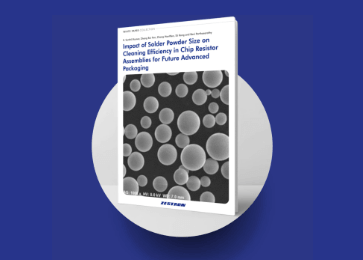
Impact of Solder Powder Size on Cleaning Efficiency in Chip Resistor Assemblies for Future Advanced PackagingOct 13, 2026Co-authored by Principal Engineer Ravi Parthasarathy, and Heraeus Presented at...