


Good news! At last week’s GSA 3D IC Packaging Working Group Meeting, July 23, 2014, Jan Vardaman uttered the words I’ve been waiting to hear her say for quite some time. “Memory stacks with TSVs are here!”
Vardaman cited three companies actively involved in new memory architectures, all of which involve stacking memory either with or without interposers – Tezzaron, Micron and Hynix. She said she’d been interviewing the companies who have engineering samples of the Hybrid Memory Cube (HMC), and the upshot of these discussions is that volume shipments will happen in 2015. That’s when she said the next thing I’ve been waiting to hear for years: “That is what I consider high volume manufacturing.” She went on to explain “you can’t shake out tools and a line until you build stuff.”
At the meeting, Vardaman offered a peek at TechSearch International’s 3D IC Gap Analysis Report that her team is putting the final touches on. Based on what I took away from her comments, while there is still work to be done, one by one the gaps to 3D IC readiness are closing. In fact, following her report were several presentations that addressed a number of the very gaps she identified.
While the drivers for going to 3D ICs have essentially remained the same, Vardaman noted that the real driver today is the high cost of lithography for next-generation silicon technology nodes. Vardaman has long held to the belief that as long as improvements keep being made to existing packaging technologies that offer a lower cost alternative to 3D ICS with TSVs, high volume manufacturing (HVM) of 3D ICs will be delayed. “The point is, people are looking for a low cost solution no matter what that is for whatever performance gain they need to have,” she explained. So essentially 3D ICs offer a lower cost solution than scaling to achieve the performance gains being sought after through, even though they are still more costly than wafer level packaging options (WLP). I couldn’t agree more.
With regard to remaining technology gaps in 3D IC readiness, Vardaman ticked off a good sized list including:
• Availability of commercial 3D EDA tools
• Micro bumping and assembly for stacked die
• Assembly of die on interposers
• The debond step in temporary bond/debond
• Thermal design and dissipation when logic is part of the stack
• Test methodology and solution
• Reliability data including drop test data
• Yield improvements that lower cost
• Infrastructure related issues such as hand-off point
On two points in particular, she went more in-depth. First was the need for path finding tools that enable the investigation of “what if” scenarios, so that technical feasibility and how to achieve best to achieve lowest unit cost can be evaluated. She said path finding allows for the exploration of alternatives for determining the optimum mix of structures and technologies. Additionally, it can help prevent the worst and most costly situation: finding errors while ramping up manufacturing.
The second area Vardaman focused on was assembly challenges. Specifically, she talked about issues with microbumping at pitches less than 50µm including under bump metallization (UBM) and mechanisms to form the bumps. Underfill materials and methods are also a concern, as its difficult to do capillary flow. She said there’s lots of promising work being done with pre-applied non-conductive pastes and films at the wafer level. Assembly of fine-pitch bumps is the challenging part, she said. Substrate warpage, thermocompression bonding, throughput, and yield are other pain points. Continued yield improvements that lower the cost are still needed, she said. “Cost is still compared to other packaging alternatives, those continue to drop in cost, so it’s not a fixed target you’re aiming for,” noted Vardaman.
Filling the EDA Gaps
The speakers from E-System Design, Mentor Graphics, Cadence Design addressed some of the EDA tool gaps Vardaman had identified including pathfinding, physical verification, electrical and thermal analysis, design for test (DFT).
“Path finding is about fast, accurate, and unrestricted exploration,” said Bill Martin, of E-Systems Design, “We are about front end planning, then go off and use all these other implementation and verification tools.”
Martin said E-System Design has been working with large companies around the world to help them understand the value of path finding, and how there are lots of different things you can do with 2.5D and 3D. (I recently met with Martin at ECTC and interviewed him about the company’s Sphinx 3D Pathfinder V3, which won the 2014 3D InCites Awards’ 3D Design Tool Award. It pretty much covers what he said in his presentation.)

John Ferguson and Dusan Petranovic, both from Mentor Graphics each presented different aspects of Calibre, Mentor’s tool for physical verification and parasitic extraction of 3D ICs.
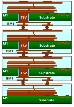
Physical verification is used to make sure we stack die properly, that the connections are formed, and the system works as expected, explained Ferguson. “Traditional tools can’t do this. They’re not up for the challenge,” he said (Figure 1). He walked the group through the Calibre 3D STACK 3D IC verification flow including physical alignment and physical verification checks, and connectivity checks. He also gave examples of success stories, working with TSMC and Tezzaron over the past few years.
Petranovic focused on extraction solutions for 3D IC stacks, comparing the advantages and challenges of various TSV modeling approaches including stand-alone TSV models, compact parametrized models, and field solver based TSV extraction.
Provided by foundries, stand-alone TSV models are easy to integrate into a flow and are sufficient in many situations, he said. However, they are not adequate for high-density, high frequency applications. In the case of compact parametrized models, TSVs and coupling models are provided by foundries. This method can account for some interactions and are faster than field-solver models, but its difficult to account for all situations and parameterize for all situations. Lastly, in field-solver based TSV extraction, TSV parasitics and their interactions are extracted. This is the most accurate modeling approach, but there are challenges with performance and integration.
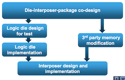
Brandon Wang, of Cadence, followed the Mentor presentations with an updated version of the presentation he gave at the DATE Conference in March. He said the Internet of Things (IOT) will add new dimension to heterogeneous integration that could be 2.5D and 3D, with or without TSVs. He also talked about the changes 3D IC brings to the EDA world. He said 2.5D/3D realization involves entire cycles with multiple 3D featured tools working together on planning, implementation, physical verification, Electrical and thermal analysis, digital signoff, and manufacture test. Wang demonstrated what he saw as a necessary 3D IC design and implementation flow (Figure 2), as well as an analysis and sign-off flow, and talked about Cadence’s 3D IC Integrated Solution.
“Silicon Designers needs to be package driven while package designers may need to leverage sophisticated silicon tools to deal massive inter-die connectivity,” said Wang. “3D-IC is more than stacking existing dies together in a package, it requires die and system level re-architecture to bring 3D-IC to production.”
By bringing the design and manufacturing community together, and building awareness around the tools that are available to achieve this, perhaps the gaps will soon be closed once and for all. ~ F.v.T


