
For the past year or so at various conferences, symposiums and summits focused on 2.5D and 3DIC technologies; we’ve been hearing suggestions about business model scenarios. It’s boiled down to three distinct choices. First is a ‘single integration’ model where end-to-end manufacturing takes place in one location – most likely a foundry or IDM. To date, the only foundry in the position to push this captive model through is TSMC, which they have been doing with their chip-on-wafer-on-substrate (CoWoS) model. The other two options are collaborative models between foundries and OSATs. In the first, the middle-end of-line (MEOL) processes take place at the foundry and the hand-off to the OSAT is a thinned wafer mounted on a temporary carrier, ready for back-end-of-line (BEOL) final assembly (stacking) and test at the OSAT; and finally a second foundry/OSAT model where the MEOL and BEOL processes are performed at the OSAT. The hand-off product in this scenario is a via-mid TSV wafer, still in thick form for easier handling.
As much as these collaborative models have been discussed and promoted, they’ve essentially existed at the theoretical level. That is, until last week’s announcement by STATS ChipPAC and UMC that the companies have successfully demonstrated the world’s first TSV-enabled 3D IC chip stacking technology developed under an open ecosystem collaboration. This project followed the second abovementioned model, with UMC handling the front-end-of-line (FEOL) steps, and then shipping the full thickness TSV wafer to STATS ChipPAC for the MEOL, BEOL, final assembly and test steps. I spoke with STATS ChipPAC’s Raj Pendse to learn more about the details and the true significance of this accomplishment for this major OSAT.
Pendse explained that ultimately, the impetus behind this work was to demonstrate that the single integration model promoted by TSMC is not the only game in town. He said that end customers were not happy with the captive model, particularly in the case of stacking memory on logic. While memory suppliers have no hesitation sending memory to an OSAT, they are not inclined to send die to a competing foundry like TSMC. But, noted Pendse, in the eyes of many customers TSMC was “playing hardball” and the customer had little choice for an alternative scenario.

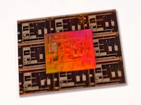
“We created this competing collaborative model to prove to the end-customer that there is an alternative,” said Pendse. The test vehicle demonstrated was a wide I/O memory test chip stacked on TSV-embedded 28nm processor test chip, and the key milestones included identifying the hand-off point and test points for determining device reliability.
What’s really interesting is that after all this concern about how to adapt the business model to handle the liability issues, what they wound up proving is that the traditional business model — where the IC vendor as the end-customer owns the liability, and the processes are outsourced to the foundry and OSAT— still rings true for 3D ICs. This is regardless of the fact that there are more potential failure points in a 3D TSV stack than in a package-on-package (PoP) device or even bare die stacks using wire bond or flip chip as the interconnect method.
“It’s more analogous to the stacked die business we do where we’re stacking bare die memory on logic using wire bond or flip chip in wafer form from two different sources,” explained Pendse. “ With TSV and particularly with wide I/O memory, we’re dealing with a more complex piece of silicon. To have that supplied in fully tested form is much more complicated than mainstream memory die. So while overall the model is still the same, it makes it harder.”
So the million-dollar question is when will product ramp to production? That’s where it gets a little complicated, and while this is a huge step forward, we’ve still got a ways to go before we see HVM of 3DICs. “Being ready on the packaging side is one thing, but there are still some roadblocks,” noted Pendse. These include design tools necessary to incorporate vias within the silicon structure. Additionally, the infrastructure for wide I/O DRAM is not quite ready. Finally, while customers want 3D ICs, Pendse says the cost adder is “still exhorbitant”. Competing solutions that achieve similar performance are being developed in the interim, and while not quite the same, Pendse says it will be adequate for the next two technology nodes; most likely after LPPDDR 4. “Given the longevity of that technology, 2015 seems earliest,” he said. That’s not to say that barriers can’t be surmounted with some effort, such as from a major OEM. “This is a dynamic landscape. Big players who want a competitive advantage can make it happen,” said Pendse.

And when it does happen, rest assured STATS ChipPAC will be ready for it. According to Pendse, the company has installed a “one-up” line consisting of one of each high volume manufacturing (HVM) tools required to perform all MEOL and BEOL processes and test. “The mid-end is new for OSATs,” he said. “We’ve set up a 300mm line in Singapore, and we’ve made a committed investment.”
While this is a production-worthy manufacturing line, Pendse says capacity won’t be added until there is a sign of growing demand. The company is marketing to the biggest players in the industry that they have the capability. “IF they are serious, it could happen quickly.” In the meantime, being prepared for 3D IC processes means they can leverage that technology and know-how to 2.5D processes. “We look at 3D being a superset of lot of different things,” said Pendse. “Having addressed the superset we can address the other things easily.”
Ultimately, what STATS ChipPAC and UMC did was to put theory into practice, and prove that an open collaborative model for 3D ICs not only works, it offers an alternative to the single integration model. It looks like TSMC is going to have some good old-fashioned healthy competition, and that’s a good thing. ~ F.v.T.


